| |
Nanodevice's group Advanced Applied Physical Science Laboratory NTT Basic Research Laboratories |
| |
Nanodevice's group Advanced Applied Physical Science Laboratory NTT Basic Research Laboratories |
| Sensing an alternating-current signal beyond the cutoff frequency using a single-electron dynamic random-access memory | |||
| Phys. Rev. Appl. p. L021001 (2025) DOI: 10.1103/PhysRevApplied.23.L021001 | |||
| C. Salhani, K. Chida, T. Shimizu, T. Hayashi, and K. Nishiguchi | |||
| [ABSTRACT] We demonstrate an alternating-current (ac) signal sensing with a nanometer-scale dynamic random access memory (DRAM) based on single-electron control. The double-gate transistor constituting the DRAM controls the motion of a single electron. When an ac signal of a frequency 6 orders of magnitude greater than the cutoff frequency of the single-electron motion through the transistor is input, single electrons are charged in the capacitor of the DRAM and subsequently read out as an output signal representing the ac signal. This ac-to-single-electron conversion is comprehensively analyzed both experimentally and theoretically from a thermodynamic perspective by our using single-electron counting statistics. Furthermore, we confirm that the response time of the ac-to-single-electron conversion is directly influenced by the cutoff frequency. These findings collectively demonstrate the potential of our single-electron DRAM as a highly sensitive sensor for high-frequency ac signals. | |||
| Sub-Femtoampere-Current Detection Using Single-Electron Sensor Operated Around 295 K | |||
| IEEE Electron Device Lett. vol. 45, pp. 1373-1376 (2024) DOI: 10.1109/LED.2024.3401237 | |||
| K. Nishiguchi and G. Yamahata | |||
| [ABSTRACT] Sub-femtoampere (sub-fA) current was detected using a device based on a dynamic random access memory (DRAM) composed of silicon-on-insulator (SOI) field-effect transistors (FETs). The device incorporated a 20-aF capacitor connected to the FETs with a two-layer gate structure, which suppressed charge leakage from and to the capacitor to the theoretical limit. The capacitor captured a small number of electrons that constitute the sub-fA current. The captured electrons, approximately 10 in number, were read out by another FET acting as a charge sensor with single-electron resolution. Consequently, a current of 100 attoamperes was detected. | |||
| Noise-to-energy conversion in a nanometer-scale dot observed with electron counting statistics | |||
| Appl. Phys. Lett. vol. 122, 213502 (2023). | |||
| K. Chida, A. Fujiwara, and K. Nishiguchi | |||
| [ABSTRACT] We converted Gaussian-distributed voltage noise applied to an electron reservoir into the non-equilibrium free energy of a nanometer-scale dot connected to the reservoir via an energy barrier. Counting statistics of single-electron motion into and out of the dot through the energy barrier allows us to quantitatively analyze the energy transported into the dot as well as changes in the internal energy and effective temperature of the dot in this noise-induced non-equilibrium steady state (NESS). By analyzing the transition rates of electrons moving into and out of the dot, we confirmed that the rectification effect caused by the asymmetry with respect to the direction of electron motion is the origin of the increase in the internal energy of the dot. The information on energy transport in a nanometer-scale dot in the noise-induced NESS obtained in this study with electron counting statistics clarifies the relationship between the non-equilibrium dynamics of a nanodevice and noise applied to it. This study provides us with the means to evaluate device operation using noise as a resource. | |||
| Room-temperature several-hundred-of-megahertz charge sensing with single-electron resolution using a silicon transistor | |||
| Appl. Phys. Lett. vol. 122, p. 043502 (2023). | |||
| K. Nishiguchi, H. Yamaguchi, A. Fujiwara, H. S. J. van der Zant, and G.A. Steele | |||
| [ABSTRACT] We demonstrate charge detection with single-electron resolution at high readout frequency using a silicon field-effect transistor (FET) integrated with double resonant circuits. A FET, whose channel of 10-nm width enables a single electron to be detected at room temperature, is connected to resonant circuits composed of coupled inductors and capacitors, and these double resonant circuits provide two resonance frequencies. When the FET is driven by a carrier signal at the lower resonance frequency, a small signal applied to the FET's gate modulates the resonance condition, resulting in a reflected signal appearing near the higher resonance frequency. Such operation utilizing the double resonant circuits enables charge detection with a single-electron resolution of 3 × 10⁻³ e/Hz0.5 and a readout frequency of 200 MHz at room temperature. In addition, a variable capacitor used in the double resonant circuits allows charge-sensing characteristics to be controlled in situ. | |||
| Seebeck effect in a nanometer-scale dot in a Si nanowire observed with electron counting statistics | |||
| Selected for Cover Art | |||
| Appl. Phys. Lett. vol. 121, p. 183501 (2022). | |||
| K. Chida, A. Fujiwara, and K. Nishiguchi | |||
| [ABSTRACT] We performed electron counting statistics to measure the thermoelectric effect in a nanometer-scale silicon dot. To separate the 100-nm-long dot from a silicon nanowire, we used an electrostatically created 30-nm-long energy barrier. By measuring current through a nearby sensor, we observed the random motion of single electrons between the dot and silicon nanowire. The statistics of single-electron motion provides us with information on temperature and voltage at the dot. Under the detailed balance assumption, we determined the temperature difference and the Seebeck voltage between the dot and silicon nanowire. The validity of our analysis was confirmed by observing the energy-barrier height dependence of the Seebeck coefficient. Furthermore, by counting the electrons leaving the dot, a minute output power on the order of sub-zeptowatt from the dot to the silicon nanowire was estimated. | |||
| (Invited) Single-Electron Manipulation in an Attofarad-Capacitor DRAM | |||
| ECS Transactions vol. 104, p. 33 (2021). | |||
| K. Nishiguchi, K. Chida, and A. Fujiwara | |||
| [ABSTRACT] We describe single-electron manipulation in a dynamic random access memory (DRAM) composed of an attofarad capacitor and nanometer-scale transistors. The motion of a single electron is controlled and then the electron is stored in the capacitor using the transistors, whose leakage current is suppressed to the theoretical limit. The charge signal of the electron is amplified by another transistor integrated in the DRAM, which functionalizes the single electron as one bit of information for data processing. In addition to such single-electron applications, power generation using a conceptual analogy of Maxwell's demon detecting and manipulating a single-electron motion is demonstrated for an understanding of the essential correlation of data processing to its energy consumption. These demonstrations are promising as a starting point for constructing new technologies for the ultimate reduction in the power consumption of data processing circuits. | |||
| Characteristics of Si Single-Electron Transistor under Illumination | |||
| ECS Trans. vol. 92, pp. 47-56 (2019). | |||
| Y. Takahashi, M. Sinohara, M. Arita, A. Tsurumaki-Fukuchi, A. Fujiwara, Y. Ono, K. Nishiguchi, and H. Inokawa | |||
| [ABSTRACT] Photo-excited carriers in Si quantum islands and their surrounded area exhibit interesting features due to electron-hole generation. We show Si single- hole transistor (SHT) characteristics in a Si single-electron transistor (SET) comprising n-type source and drain electrodes under illumination. Holes excited in the Si are expected to flow through the SET island by applying negative gate voltages. Interesting phenomenon is the co-existence of electrons and holes around the island. In a SET, when holes generated by photo-excitation are trapped in the one side (either top or bottom side) of the SET island under the vertical electric field, the SET characteristics are changed depending on the number of trapped holes because effective total number of electrons can be negative. Here, we show the characteristics of photo-excited SETs without strong vertical electric fields. | |||
| Power generator driven by Maxwell’s demon | |||
| Nature Commun. vol. 8, p. 15310 (2017). | |||
| K. Chida, S. Desai, K. Nishiguchi, and A. Fujiwara | |||
| [ABSTRACT] Maxwell’s demon is an imaginary entity that reduces the entropy of a system and generates free energy in the system. About 150 years after its proposal, theoretical studies explained the physical validity of Maxwell’s demon in the context of information thermodynamics, and there have been successful experimental demonstrations of energy generation by the demon. The demon’s next task is to convert the generated free energy to work that acts on the surroundings. Here, we demonstrate that Maxwell’s demon can generate and output electric current and power with individual randomly moving electrons in small transistors. Real-time monitoring of electron motion shows that two transistors functioning as gates that control an electron’s trajectory so that an electron moves directionally. A numerical calculation reveals that power generation is increased by miniaturizing the room in which the electrons are partitioned. These results suggest that evolving transistor-miniaturization technology can increase the demon’s power output. | |||
| Fabrication and single-electron-transfer operation of a triple-dot single-electron transistor | |||
| J. Appl. Phys. vol. 118, p. 214305 (2015). | |||
| M. Jo, T. Uchida, A. Tsurumaki-Fukuchi, M. Arita, A. Fujiwara, Y. Ono, K. Nishiguchi, H. Inokawa, and Y. Takahashi | |||
| [ABSTRACT] A triple-dot single-electron transistor was fabricated on silicon-on-insulator wafer using pattern-dependent oxidation. A specially designed one-dimensional silicon wire having small constrictions at both ends was converted to a triple-dot single-electron transistor by means of pattern-dependent oxidation. The fabrication of the center dot involved quantum size effects and stress-induced band gap reduction, whereas that of the two side dots involved thickness modulation because of the complex edge structure of two-dimensional silicon. Single-electron turnstile operation was confirmed at 8 K when a 100-mV, 1-MHz square wave was applied. Monte Carlo simulations indicated that such a device with inhomogeneous tunnel and gate capacitances can exhibit single-electron transfer. | |||
| Thermal-noise suppression in nano-scale Si field-effect transistors by feedback control based on single-electron detection | |||
| Appl. Phys. Lett. vol. 107, p. 073110 (2015). | |||
| K. Chida, K. Nishiguchi, G. Yamahata, H. Tanaka, and A. Fujiwara | |||
| [ABSTRACT] We perform feedback (FB) control for suppressing thermal fluctuation in the number of electrons in a silicon single-electron (SE) device composed of a small transistor and capacitor. SEs enter and leave the capacitor via the transistor randomly at thermal equilibrium, which is monitored in real time using a high-charge-sensitivity detector. In order to suppress such random motion or thermal fluctuation of the electrons, SEs are injected and removed using the transistor according to the monitored change in the number of electrons in the capacitor, which is exactly the FB control. As a result, thermal fluctuation in the number of electrons in a SE device is suppressed by 60%, which corresponds to the so-called FB cooling from 300 to 110 K. Moreover, a thermodynamics analysis of this FB cooling reveals that entropy in the capacitor is reduced and the device is at non equilibrium; i.e., the free energy of the device increases. Since this entropy reduction originates from information about the electrons’ motion monitored by the detector, our results by the FB control represent one type of information-to-energy conversion. | |||
| Deviation from the law of energy equipartition in a small dynamic-random-access memory | |||
| Jpn. J. Appl. Phys. vol. 54, 06FG03 (2015). | Single-electron detection of thermal noise 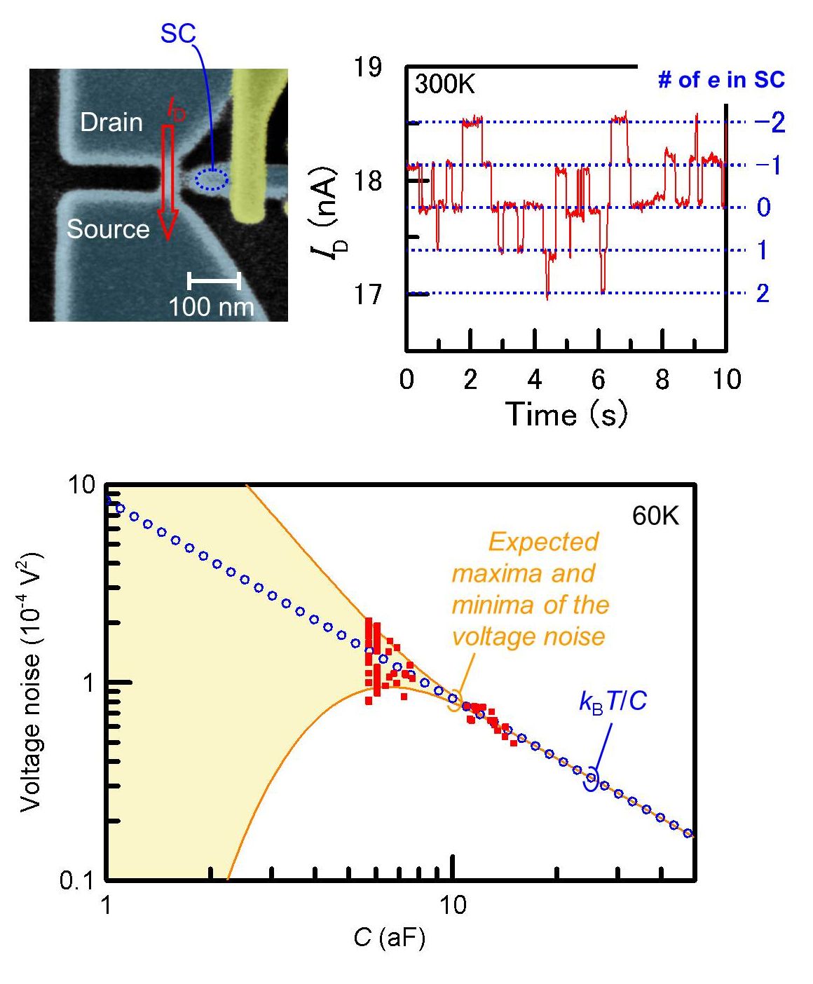 | ||
| P. A. Carles, K. Nishiguchi, and A. Fujiwara | |||
| [ABSTRACT] A small dynamic-random-access memory (DRAM) coupled with a high charge sensitivity electrometer based on a silicon field-effect transistor is used to study the law of equipartition of energy. By statistically analyzing the movement of single electrons in the DRAM at various temperature and voltage conditions in thermal equilibrium, we are able to observe a behavior that differs from what is predicted by the law of equipartition energy: when the charging energy of the capacitor of the DRAM is comparable to or smaller than the thermal energy kBT/2, random electron motion is ruled perfectly by thermal energy; on the other hand, when the charging energy becomes higher in relation to the thermal energy kBT/2, random electron motion is suppressed which indicates a deviation from the law of equipartition of energy. Since the law of equipartition is analyzed using the DRAM, one of the most familiar devices, we believe that our results are perfectly universal among all electronic devices. | |||
| Gigahertz single-trap electron pumps in silicon | |||
| Nat. Commun. vol. 5, p. 5038 (2014). | |||
| G. Yamahata, K. Nishiguchi, and A. Fujiwara | |||
| [ABSTRACT] Manipulation of single electrons is the key to developing ultimate electronics such as single-electron-based information processors and electrical standards in metrology. Especially, high-frequency and high-accuracy single-electron pumps are essential to realize practical current standards. While electrically defined quantum dots are widely used to build single-electron pumps, a localized state in semiconductors is also a potential candidate for accurate pumps because it can have a large activation energy for the captured electron. However, the transfer mechanism of such localized-state-mediated single-electron pumps for high-accuracy operation at a high frequency has not been well examined. Here we demonstrate a single-electron pump using a single-trap level with an activation energy of a few ten millielectron volts in Si nanotransistors. By means of gate control of capture and emission rates, the pump operates at a frequency of 3 GHz with an accuracy of better than 10^−3 at 17 K, indicating that an electric field at the trap level lowers the capture and emission time to less than 25 ps. | |||
| Single-electron thermal noise | |||
|
Picked up in LAB TALK of nanotechweb.org and Nanotechnology. Picked up in IOPselect. | |||
| Nanotechnology vol. 25, p. 275201 (2014). | Single-electron detection of thermal noise 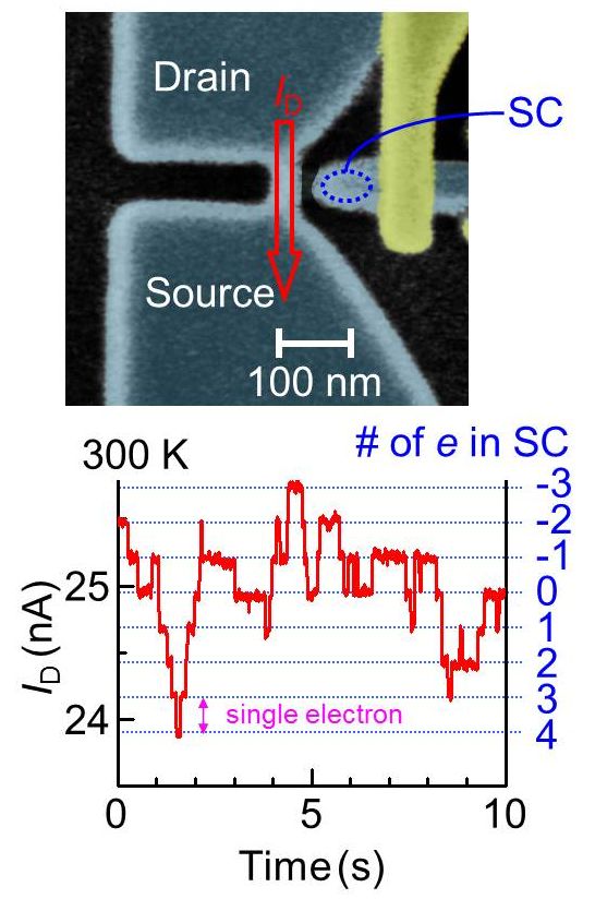 | ||
| K. Nishiguchi, Y. Ono, and A. Fujiwara | |||
| [ABSTRACT] We report the observation of thermal noise on the motion of single electrons in an ultimately small dynamic random access memory (DRAM). Nanometer-scale transistors composing the DRAM resolve the thermal noise in single-electron motion. A complete set of fundamental tests conducted on this single-electron thermal noise shows that this noise perfectly follows all the aspects predicted by the statistical mechanics, which include the occupation probability, the law of equipartition, a detailed balance, and the law of kT/C. In addition, the counting statistics on the directional motion, i.e., the current, of the single-electron thermal noise indicate that the individual electron motion follows the Poisson process like in shot noise. | |||
| Accuracy evaluation and mechanism crossover of single-electron transfer in Si tunable-barrier turnstiles | |||
| Phys. Rev. B, vol. 89, p. 165302 (2014). | |||
| G. Yamahata, K. Nishiguchi, and A. Fujiwara | |||
| [ABSTRACT] Using an error-counting scheme, we evaluated the accuracy of single-electron (SE) transfer in Si tunable-barrier turnstiles in a dilution refrigerator. The error counting was performed by shuttling SEs between a lead and a charge-accumulating node and detecting in real time the number of electrons in the node with an SE-resolution charge sensor. The best experimentally obtained error rate is about 100 parts per million (ppm), where the SE capture in the SE island occurs in thermal equilibrium due to the heating effect on SEs caused by pulse voltages applied to modulate the potential barrier. When we reduce the heating effect by suppressing the pulse voltages, there is a change in the SE transfer mechanism to nonequilibrium SE capture. We theoretically discuss the crossover point of the change. Moreover, at the minimum pulse voltage, the theoretical lower bound of the error rate estimated by fitting is on the order of 0.01 ppm. This suggests that Si SE-transfer devices are promising candidates for use as quantum current standards in metrology. | |||
| Wide-bandwidth charge sensitivity with a radio-frequency field-effect transistor | |||
| Appl. Phys. Lett. vol. 103, p. 143102 (2013). | Fast charge sensing using an FET combined with an LC circuit 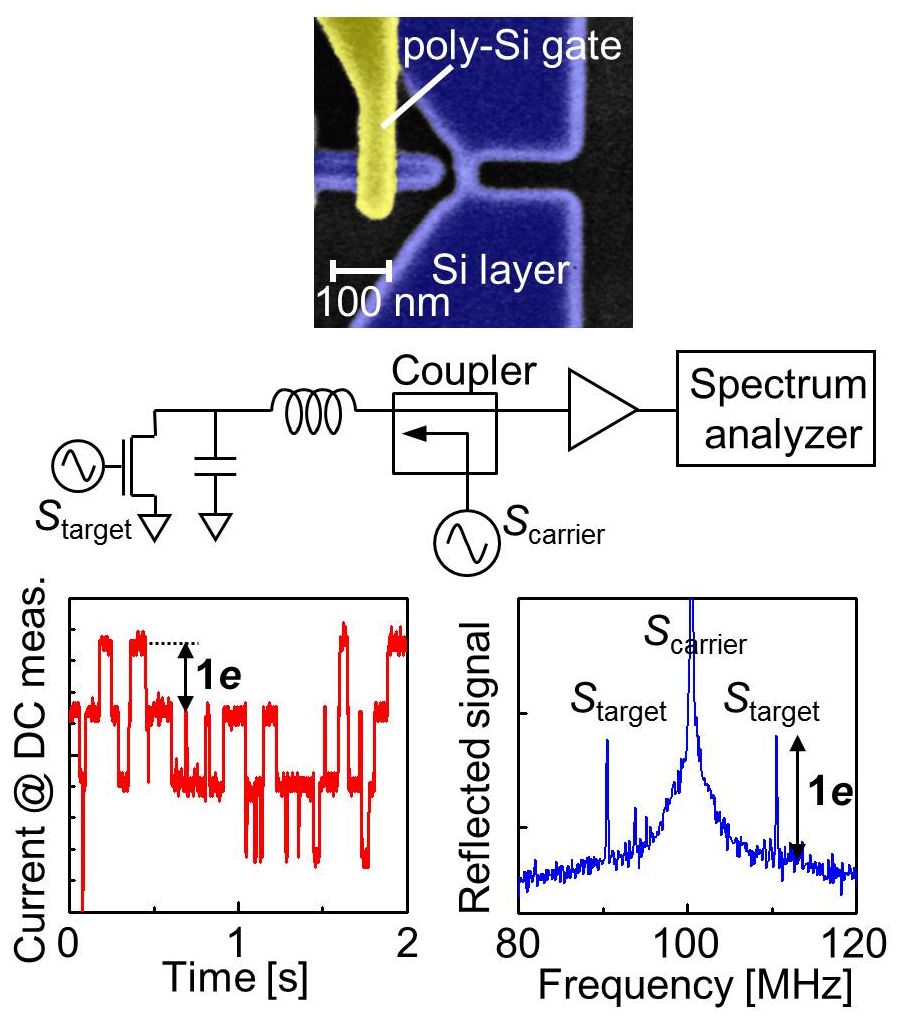 | ||
| K. Nishiguchi, H. Yamaguchi, A. Fujiwara, H. S. J. Zant, and G. A. Steele | |||
| [ABSTRACT] We demonstrate high-speed charge detection at room temperature with single-electron resolution by using a radio-frequency field-effect transistor (RF-FET). The RF-FET combines a nanometer-scale silicon FET with an impedance-matching circuit composed of an inductor and capacitor. Driving the RF-FET with a carrier signal at resonance frequency, small signals at the transistor’s gate modulate the resonance condition, which is monitored at high speed using the reflected signal. The RF-FET driven by high-power carrier signals enables a charge sensitivity of 2×10^-4 e/Hz^0.5 at readout band-width of 20 MHz. | |||
| Single-Electron Stochastic Resonance Using Si Nanowire Transistors | |||
| Picked up in SPOTLIGHTS: Editors'Choice from APEX and JJAP. | |||
| Jpn. J. Appl. Phys., vol. 50, p. 06GF04 (2011). | Patern perception using stochastic resonace  |
||
| K. Nishiguchi and A. Fujiwara | |||
| [ABSTRACT] We demonstrate stochastic resonance (SR) with single electrons (SEs) using nanoscale metal-oxide-semiconductor field-effect transistors (MOSFETs). Input signal applied to a MOSFET modulates SE transport in an average manner based on nonlinear characteristics. On the other hand, an individual SE goes through the MOSFET in a completely random manner, which corresponds to shot noise. SEs transferred to a storage node are counted precisely by the other MOSFET and used as an output signal. The correlation between the input and output signals is improved by taking advantage of extrinsic noise as well as the intrinsic shot noise composed of SEs. It is confirmed that the shot-noise-assisted SR allows fast operation with a simple system. Pattern perception utilizing SR is also demonstrated. | |||
| Single-electron counting statistics of shot noise in nanowire Si metal-oxide-semiconductor field-effect transistors | |||
| Picked up in the May 23, 20011 issue of Virtual Journal of Nanoscale Science & Technology | |||
| Appl. Phys. Lett., vol. 98, p. 193502 (2011). | Time-domain analysis on shot noise 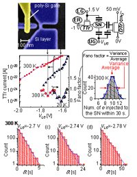 | ||
| K. Nishiguchi, Y. Ono, and A. Fujiwara | |||
| [ABSTRACT] Shot noise in the transport of single electrons in a Si metal-oxide-semiconductor field-effect transistor is monitored by real-time measurement with a high-charge-sensitivity electrometer. In the current range between zepto and attoamperes, the current characteristics are found to be divided into two regimes: a temperature-independent regime in the lower current range and a temperature-dependent one in the higher current range. A time-domain analysis reveals that, for both regimes, the single-electron transport obeys a pure Poisson process with the Fano factor’s being nearly unity, while the shot noise is suppressed with reduced Fano factors around the boundary. c 2011 American Institute of Physics | |||
| Accuracy evaluation of single-electron shuttle transfer in Si nanowire metal-oxide-semiconductor field-effect transistors | |||
| Appl. Phys. Lett., vol. 98, p. 222104 (2011). | |||
| G. Yamahata, K. Nishiguchi, and A. Fujiwara | |||
| [ABSTRACT] We report on evaluation of transfer accuracy in a single-electron turnstile using silicon nanowire metal-oxide-semiconductor field-effect transistors at 17 K. Single-electron shuttle transfer and single-shot detection of a single electron are used to detect errors of the transfer. Errors for the transfer through an electrostatically formed island are ascribed to thermal processes. We also observed single-electron transfer mediated by a trap level, which exhibits a wide current plateau and a low error rate. c 2011 American Institute of Physics | |||
| Resonant escape over an oscillating barrier in a single-electron ratchet transfer | |||
| Phys. Rev. B, vol. 82, p. 033303 (2010). | |||
| S. Miyamoto, K. Nishiguchi, Y. Ono, K. M. Itoh, and A. Fujiwara | |||
| [ABSTRACT] Single-electron escape from a metastable state over an oscillating barrier is experimentally investigated in silicon-based ratchet transfer. When the barrier is oscillating on a time-scale characteristic of the single-electron escape, synchronization occurs between the deterministic barrier modulation and the stochastic escape events. The average escape time as a function of its oscillation frequency exhibits a minimum providing a primary signature for resonant activation of single electrons. c 2010 The American Physical Society | |||
| Single-electron counting statistics and its circuit application in nanoscale field-effect transistors at room temperature | |||
| Nanotechnology, vol. 20, p. 175201 (2009). | Flexible pattern recognition | ||
| K. Nishiguchi and A. Fujiwara | |||
| [ABSTRACT] A circuit utilizing single electrons is demonstrated at room temperature. Individual electrons randomly passing through the nanoscale silicon-on-insulator metal-oxide-semiconductor field-effect transistor (MOSFET) are monitored by an electrometer in real time. Such a random behavior of single electrons is used for high-quality random-number generation suitable for data processing which stochastically extracts the most preferable pattern among various ones. MOSFET-based random-number generation allows fast operation as well as high controllability, which leads to flexible extraction of the preferable pattern. | |||
| Horizontal position analysis of single acceptors in Si nanoscale field-effect transistors | |||
| Appl. Phys. Lett., vol. 94, 223501 (2009) | |||
| M. A. H. Khalafalla, Y. Ono, K. Nishiguchi, and A. Fujiwara | |||
| [ABSTRACT] The authors performed conductance measurements to identify the horizontal position of single boron acceptors in silicon-on-insulator nanoscale field-effect transistors at a temperature of 6 K. The horizontal position, i.e., how far the acceptor is from the source or drain terminal, is qualitatively obtained, and it is shown, on the level of single dopants, that the acceptor near the source significantly affects the subthreshold nature of the transistor. c 2009 American Institute of Physics | |||
| Single-Electron-Resolution Electrometer Based on Field-Effect Transistor | |||
| Picked up in the December 15, 2008 issue of Virtual Journal of Nanoscale Science & Technology | |||
| Jpn. J. Appl. Phys., vol. 47, pp. 8305-8310 (2008). | Single-electron detection at room temperature 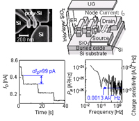 | ||
| K. Nishiguchi, C. Koechlin, Y. Ono, A. Fujiwara, H. Inokawa, and H. Yamaguchi | |||
| [ABSTRACT] An electrometer based on field-effect transistors (FETs) was fabricated on a silicon-on-insulator substrate (SOI). The electrometer has a nanometer-scale small channel and a capacitively coupled node, where single electrons are stored. We discuss the dependence of the charge sensitivity of the electrometer on its structure and on its operation condition and gives guides for achieving the higher charge sensitivity. The device optimization based on this dependence allows the demonstration of the electrometer with extremely high charge sensitivity, 0.0013 e/√Hz at 1 Hz, at room temperature. | |||
| Stochastic data processing circuit based on single electrons using nanoscale field-effect transistors | |||
| Picked up in the February 25, 2008 issue of Virtual Journal
of Nanoscale Science & Technology. Picked up in News and Views of the May 8, 2008 online issue of Nature. | |||
| Appl. Phys. Lett., vol. 92, p. 062105 (2008). | Flexible logic circuit | ||
| K. Nishiguchi, Y. Ono, A. Fujiwara, H. Inokawa, and Y. Takahashi | |||
| [ABSTRACT] A circuit utilizing single electrons is demonstrated at room temperature using a silicon-on-insulator metal-oxide-semiconductor field-effect transistor (MOSFET). Individual electrons randomly passing through the nanoscale MOSFET, which are the origin of shot noise, are monitored by an electrometer in real time. This random behavior of single electrons is used as a random number for a stochastic associative memory for image-pattern matching, in which the most preferable pattern is extracted with the largest probability. The use of electron transport in the MOSFET provides high controllability of the randomness as well as fast generation of random numbers. The present result promises single-electron applications using nanoscale MOSFETs. c 2008 American Institute of Physics | |||
| Escape dynamics of a few electrons in a single-electron ratchet using silicon nanowire metal-oxide-semiconductor field-effect transistor | |||
| Appl. Phys. Lett., vol. 93, 222103 (2008) | |||
| S. Miyamoto, K. Nishiguchi, Y. Ono, K M. Itoh, and A. Fujiwara. | |||
| [ABSTRACT] Transport dynamics of a few electrons in a quantum dot are investigated in a single-electron ratchet using silicon nanowire metal-oxide-semiconductor field-effect transistors. Time-resolved measurements in a nanosecond regime are carried out to determine the escape times of the first, second, and third electrons from the quantum dot originally containing three electrons. The escape time strongly depends on the number of electrons due to the single-electron charging effect in the quantum dot, which makes it possible to achieve selective ejection of a desired number of electrons. c 2008 American Institute of Physics | |||
| Silicon single-charge transfer devices | |||
| J. Phys. Chem. Solids Vol. 69, No. 2-3, 702-707 (2008) | |||
| Y. Ono, A. Fujiwara, K. Nishiguchi, Y. Takahashi, and H. Inokawa. | |||
| [ABSTRACT] The single-electron device (SED) enables the control of electron motion on the level of an elementary charge. Single-charge transfer devices are special SEDs that enable single-electron transfer synchronized with the gate clock. They have the potential for extremely low transfer error rates and are expected to be building blocks for future information processing and electrical metrology. We have been pursuing the fabrication of Si-based SEDs using CMOS technology with the help of electron-beam lithography and have recently demonstrated the single-charge transfer devices. The devices are composed of one Si quantum dot sandwitched between two tiny MOS gates and can operate at much higher temperatures than those of former metal-based and compound-semiconductor-based devices. This opens up the possibility of the practical use of clocked single-charge transfer. | |||
| Nanoampere charge pump by single-electron ratchet using silicon nanowire metal-oxide-semiconductor field-effect transistor | |||
| Appl. Phys. Lett., vol. 92, 042102 (2008) | |||
| A. Fujiwara, K. Nishiguchi, and Y. Ono. | |||
| [ABSTRACT] Nanoampere single-electron pumping is presented at 20 K using a single-electron ratchet comprising silicon nanowire metal-oxide-semiconductor field-effect transistors. The ratchet features an asymmetric potential with a pocket that captures single electrons from the source and ejects them to the drain. Directional single-electron transfer is achieved by applying one ac signal with the frequency up to 2.3 GHz. We find anomalous shapes of current steps which can be ascribed to nonadiabatic electron capture. c 2008 American Institute of Physics | |||
| Identification of single and coupled acceptors in silicon nano-field-effect transistors | |||
| Appl. Phys. Lett., vol. 12, 263513 (2007) | |||
| M. A. H. Khalafalla, Y. Ono, K. Nishiguchi, and A. Fujiwara. | |||
| [ABSTRACT] We performed dopant mediated hole transport measurements to identify the depth position of individual boron acceptors and investigate two-acceptor coupling in silicon-on-insulator nanoscale field-effect transistors at a temperature of 6 K. The depth position is qualitatively obtained from the analysis of the acceptor-to-gate capacitances. We also observe signatures of a two-acceptor capacitive coupling in the characteristics of the conductance versus the front and back gate voltages. c 2007 American Institute of Physics | |||
| Transfer and detection of single electrons using metal-oxide-semiconductor field-effect transistors | |||
| IEICE Trans. Electron., vol. E90-C, p. 943 (2007). | |||
| W. Zhang, K. Nishiguchi, Y. Ono, A. Fujiwara, H. Yamaguchi, H. Inokawa, Y. Takahashi, and N. J. Wu. | |||
| [ABSTRACT] A single-electron turnstile and electrometer circuit was fabricated on a silicon-on-insulator substrate. The turnstile, which is operated by opening and closing two metal-oxide-semiconductor field-effect transistors (MOSFETs) alternately, allows current quantization at 20 K due to single-electron transfer. Another MOSFET is placed at the drain side of the turnstile to form an electron storage island. Therefore, one-by-one electron entrance into the storage island from the turnstile can be detected as an abrupt change in the current of the electrometer, which is placed near the storage island and electrically coupled to it. The correspondence between the quantized current and the single-electron counting was confirmed. | |||
| Conductance modulation by individual acceptors in Si nanoscale field-effect transistors | |||
| Appl. Phys. Lett., vol. 90, 102106 (2007). | |||
| Y. Ono, K. Nishiguchi, A. Fujiwara, H. Yamaguchi, H. Inokawa, and Y. Takahashi. | |||
| [ABSTRACT] The authors measured low-temperature conductance in nanoscale p-channel field-effect transistors lightly doped with boron. They observed a conductance modulation, which they ascribed to the trapping/detrapping of single holes by/from individual acceptors. The statistics of the appearance of the modulation in a few ten samples indicates that the number of acceptors is small, or even just one, suggesting that what the authors have observed is single-charge-transistor operation by a single-acceptor quantum dot. c 2007 American Institute of Physics | |||
| Room-temperature-operating data processing circuit based on single-electron transfer and detection with metal-oxide-semiconductor field-effect transistor technology | |||
| Picked up in the May 15, 2006 issue of Virtual Journal
of Nanoscale Science & Technology Picked up in the June 29, 2006 online issue of Nature Nanotechnology. | |||
| Appl. Phys. Lett., vol. 88, p. 183101 (2006). | Digital-Analog Converter using single electrons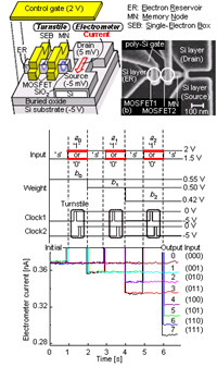 | ||
| K. Nishiguchi, A. Fujiwara, Y. Ono, H. Inokawa, and Y. Takahashi | |||
| [ABSTRACT] A single-electron-based circuit, in which electrons are transferred one by one with a turnstile and subsequently detected with a high-charge-sensitivity electrometer, was fabricated on a silicon-on-insulator substrate. The turnstile, which is operated by opening and closing two metal-oxide-semiconductor field-effect transistors alternately, allows single-electron transfer at room temperature owing to electric-field-assisted shrinkage of the single-electron box. It also achieves fast single-electron transfer (less than 10 ns) and extremely long retention (more than 10^4 s). We have applied these features to a multilevel memory and a time-division weighted sum circuit for a digital-to-analog converter. c 2006 American Institute of Physicsys | |||
| Impurity conduction in phosphorus-doped buried-channel silicon-on-insulator field-effect transistors at temperatures between 10 and 295 K | |||
| Phys. Rev. B, vol. 74, p. 235317 (2006) | |||
| Y. Ono, J-F Morizur, K. Nishiguchi, K. Takashina, and H. Yamaguchi | |||
| [ABSTRACT] We investigate transport in phosphorus-doped buried-channel metal-oxide-semiconductor field-effect transistors at temperatures between 10 and 295 K. We focus on transistors with phosphorus donor concentrations higher than those previously studied, where we expect conduction to rely on donor electrons rather than conduction-band electrons. In a range of doping concentration between around 2.1 and 8.7×10^17 cm^-3, we find that a clear peak emerges in the conductance versus gate-voltage curves at low temperature. In addition, temperature dependence measurements reveal that the conductance obeys a variable-range-hopping law up to an unexpectedly high temperature of over 100 K. The symmetric dual-gate configuration of the silicon-on-insulator we use allows us to fully characterize the vertical-bias dependence of the conductance. Comparison to computer simulation of the phosphorus impurity band depth profile reveals how the spatial variation of the impurity-band energy determines the hopping conduction in transistor structures. We conclude that the emergence of the conductance peak and the high-temperature variable-range hopping originate from the band bending and its change by the gate bias. Moreover, the peak structure is found to be strongly related to the density of states (DOS) of the phosphorus impurity band, suggesting the possibility of performing a spectroscopy for the DOS of phosphorus, the dopant of paramount importance in Si technology, through transport experiments. c 2006 The American Physical Society | |||
| Back-Gate Effect to Coulomb Blockade in Silicon-on-Insulator Trench Wires | |||
| Jpn. J. Appl. Phys., vol. 44, pp. 7717-7719 (2005). | |||
| K. Nishiguchi, C. Olivier, H. Namatsu, S. Horiguchi, Y. Ono, A. Fujiwara, Y. Takahashi, and H. Inokawa | |||
| [ABSTRACT] A back-gate (BG) effect on a Coulomb blockade in a double-gate silicon-on-insulator (SOI) nanowire is investigated. The nanowire, which is situated at the bottom of a trench and connected to thicker source/drain regions, has a naturally formed barrier at both ends and works as a single-electron transistor at low temperatures. We found that a negative BG voltage increases the charging energy of the Coulomb-blockade island in the nanowire as well as the tunnel resistance of the barriers. This indicates the possibility that the BG voltage shifts the electron wave functions in the source/drain area away from the Coulomb-blockade island and decreases the capacitance of the small junctions located at both ends of the island. | |||
| Manipulation and detection of single electrons for future information processing | |||
| J. Appl. Phys., vol. 97, p. 031101 (2005). | |||
| Y. Ono, A. Fujiwara, K. Nishiguchi, H. Inokawa, and Y. Takahashi | |||
| [ABSTRACT] The ultimate goal of future information processing might be the realization of a circuit in which one bit is represented by a single electron. Such a challenging circuit would comprise elemental devices whose tasks are to drag, transfer, and detect single electrons. In achieving these tasks, the Coulomb blockade, which occurs in tiny conducting materials, plays an important role. This paper describes the current status of research on such single-charge-control devices from the viewpoints of circuit applications. c 2005 American Institute of Physics | |||
| Multifunctional Boolean Logic Using Single-Electron Transistors | |||
| IEICE Trans. Electron., vol. E87-C, pp. 1809-1817 (2004). | Full adder circuit using single-electron transistors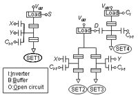 | ||
| K. Nishiguchi, H. Inokawa, Y. Ono, A. Fujiwara, and Y. Takahashi | |||
| [ABSTRACT] A multifunctional Boolean logic circuit composed of single-electron transistors (SETs) was fabricated and its operation demonstrated. The functions of Boolean logic can be changed by the half-period phase shift of the Coulomb-blockade (CB) oscillation of some SETs in the circuit, and an automatic control based on a feedback process is used to attain an exact shift. The amount of charges in the memory node (MN), which is capacitively coupled to the SET, controls the phase of the CB oscillation, and the output signal of the SET controls the amount of charge in the MN during the feedback process. This feedback process automatically adjusts SET output characteristics in such a way that it is used for the multifunctional Boolean logic. We experimentally demonstrated the automatic phase control and examined the speed of the feedback process by SPICE circuit simulation combined with a compact analytical SET model. The simulation revealed that programming time could be of the order of a few ten nanoseconds, thereby promising high-speed switching of the functions of the multifunctional Boolean logic circuit. | |||
| Multilevel memory using an electrically formed single-electron box | |||
| Picked up in August 23, 2004 issue of Virtual Journal of Nanoscale Science & Technology. | |||
| Appl. Phys. Lett., vol. 85, pp. 1277-1279 (2004). | Multileval memory represented by single electrons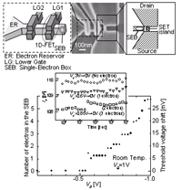 | ||
| K. Nishiguchi, H. Inokawa, Y. Ono, A. Fujiwara, and Y. Takahashi | |||
| [ABSTRACT] A multilevel dynamic random-access memory using a single-electron box (SEB) and single-electron transistor (SET) is fabricated on a silicon-on-insulator substrate. A one-dimensional field-effect transistor (FET), which is connected to the SEB, modulates a barrier potential to precisely control the number of electrons one by one in the SEB by means of the Coulomb-blockade phenomenon. At room temperature and 26 K, we demonstrate a multilevel memory, in which each interval between the levels is given by a single electron, by using the SET electrometer coupled capacitively to the SEB. The control of stored electrons by the FET assures long-retention time and high-speed write/erase operation. | |||
| Multilevel memory using single-electron turnstile | |||
| Electron. Lett., vol. 40, pp. 229-230 (2004). | Single-electron transfer and detection 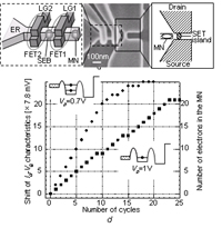 | ||
| K. Nishiguchi, H. Inokawa, Y. Ono, A. Fujiwara, and Y. Takahashi | |||
| [ABSTRACT] A multilevel single-electron memory has been successfully demonstrated. Two fine gates with phase-shifted pulse voltages modulate potential barriers in a one-dimensional Si channel to transfer electrons one by one into a memory node, and the number of electrons in the node is sensed by a single-electron transistor. | |||
| Automatic Control of Oscillation Phase of a Single-Electron Transistor | |||
| IEEE Electron Device Lett. vol. 25, pp. 31-33 (2004). | Control of Coulomb blockade osscilation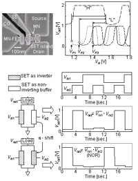 | ||
| K. Nishiguchi, H. Inokawa, Y. Ono, A. Fujiwara, and Y. Takahashi | |||
| [ABSTRACT] Automatic phase control of the Coulomb-blockade (CB) oscillation of a single-electron transistor (SET) is proposed and experimentally demonstrated. Charges in the memory node (MN) capacitively coupled to the SET control the phase of the CB oscillation. The output signal of the SET can controls chares in the MN. This feedback mechanism automatically adjusts the amount of charges, so that the output signal is leveled with a requested one for arbitrary input signal of the SET. The electrical phase control realizes the demonstration of a multifunctional Boolean logic. | |||