| |
Nanodevice's group Advanced Applied Physical Science Laboratory NTT Basic Research Laboratories |
| |
Nanodevice's group Advanced Applied Physical Science Laboratory NTT Basic Research Laboratories |
| Scalable Parallel Single-Electron Pumps in Silicon with Split-Source Control in the Nanoampere Regim | |||
| Nano Lett. vol. 25, pp. 10202-10208 (2025) DOI: 10.1021/acs.nanolett.5c02327 | |||
| G. Yamahata, T. Shimizu, K. Nishiguchi, and A. Fujiwara | |||
| [ABSTRACT] Parallelizing single-electron pumps offers a promising route to achieving nanoampere-level currents crucial for quantum current standard applications. Achieving such current levels is essential for demonstrating the ultrahigh accuracy of single-electron pumps below 0.1 ppm toward quantum metrology triangle experiments. In addition, improving the accuracy at this current range is also desirable for practical small-current measurements. However, nanoampere-level currents have not yet been achieved with parallel pumps, mainly due to challenges in optimizing operating conditions. Here, we propose a scalable and easily implementable parallelization method based on tunable-barrier single-electron pumps with split source electrodes. By tuning the source voltages, we successfully parallelize four single-electron pumps at 200 MHz and further demonstrate a current plateau exceeding 2 nA using three pumps at 2.1 GHz. The wide applicability of this parallelization technique opens a path toward advancing high-accuracy quantum current standards. | |||
| Effective Medium Approximation for Variable-Range Hopping | |||
| J. Phys. Soc. Jpn. vol. 94, p. 044001 (2025) DOI: 10.7566/JPSJ.94.044001 | |||
| T. Hayashi, Y. Tokura, and K. Nishiguchi | |||
| [ABSTRACT] The effective medium approximation is extended to include variable-range hopping transport. Homogeneous pair conductances are assigned not only to nearest-neighbor pairs of sites but also to pairs of remote sites. The conductance through a random resistor network is calculated on the basis of both rate equations and the extended effective medium approximation. By comparing their results, it is deduced that the development of long-range ordering in the spatial distribution of voltage potentials is necessary to observe variable-range hopping transport. | |||
| Electron thermometry for Si MOS inversion layer using proximity nano-transistor and its application to Joule-heating experiment | |||
| Appl. Phys. Lett. vol. 126, p. 083501 (2025) DOI: 10.1063/5.0239500 | |||
| H. M. Nayem, M. Hori, K. Nishiguchi, and Y. Ono | |||
| [ABSTRACT] A method for measuring the electron temperature in the inversion layer of Si metal-oxide-semiconductor structures is presented. This technique utilizes a nano-transistor as a thermometer, placed in close proximity to the inversion layer under investigation, enabling measurements of the electron temperature for values above approximately 10 K. When applied to Joule-heating experiments, this method reveals a notable discrepancy between the measurement results and predictions made by the conventional theory based on the deformation-potential coupling with low-energy acoustic phonons. Specifically, the injected-power dependence of the electron temperature is much weaker than expected. The results strongly suggest that another mechanism causing a significant electron energy loss plays a role. | |||
| Sensing an alternating-current signal beyond the cutoff frequency using a single-electron dynamic random-access memory | |||
| Phys. Rev. Appl. vol. 23, p. L021001 (2025) DOI: 10.1103/PhysRevApplied.23.L021001 | |||
| C. Salhani, K. Chida, T. Shimizu, T. Hayashi, and K. Nishiguchi | |||
| [ABSTRACT] We demonstrate an alternating-current (ac) signal sensing with a nanometer-scale dynamic random access memory (DRAM) based on single-electron control. The double-gate transistor constituting the DRAM controls the motion of a single electron. When an ac signal of a frequency 6 orders of magnitude greater than the cutoff frequency of the single-electron motion through the transistor is input, single electrons are charged in the capacitor of the DRAM and subsequently read out as an output signal representing the ac signal. This ac-to-single-electron conversion is comprehensively analyzed both experimentally and theoretically from a thermodynamic perspective by our using single-electron counting statistics. Furthermore, we confirm that the response time of the ac-to-single-electron conversion is directly influenced by the cutoff frequency. These findings collectively demonstrate the potential of our single-electron DRAM as a highly sensitive sensor for high-frequency ac signals. | |||
| First-Principles Investigation of the Valley Splitting of Si Quantum Slabs | |||
| Physica Status Solidi. B. p. 2400531 (2024) DOI: 10.1002/pssb.202400531 | |||
| T. Hayashi, H. Kageshima, Y. Tokura, J. Noborisaka, and K. Nishiguchi | |||
| [ABSTRACT] First-principles calculations based on density functional theory are performed on silicon (Si) quantum slabs to investigate the valley splitting of the lowest sub-bands at the Γ point in the conduction band. The calculations show that strong strain in the [110] direction of the slab largely enhances the valley splitting, which may be related to the giant valley splitting observed in a device consisting of silicon-on-insulator and buried oxide layers. The relation between the valley splitting and the atomic configuration of the slabs is also examined. | |||
| Valley splitting by extended zone effective mass approximation incorporating strain in silicon | |||
| J. Appl. Phys. vol. 135, p. 204302 (2024) DOI: 10.1063/5.0173578 | |||
| J. Noborisaka, T. Hayashi, A. Fujiwara, and K. Nishiguchi | |||
| [ABSTRACT] We propose a main mechanism of large valley splitting experimentally observed at the interface of buried oxide (BOX)/silicon-on-insulator (SOI) structures. Silicon metal-oxide-semiconductor field effect transistors fabricated on a SIMOX (001) substrate, which is a kind of the SOI substrate, that is annealed at high temperatures for a long time are known to exhibit large valley splitting, but the origin of this splitting has long been unknown. Extended zone effective-mass approximation predicts that strain significantly affects valley splitting. In this study, we analyzed valley splitting based on this theory and found that the shear strain along [110] of approximately 5% near the BOX interface is a promising source for large valley splitting. | |||
| Sub-Femtoampere-Current Detection Using Single-Electron Sensor Operated Around 295 K | |||
| IEEE Electron Device Lett. vol. 45, pp. 1373-1376 (2024) DOI: 10.1109/LED.2024.3401237 | |||
| K. Nishiguchi and G. Yamahata | |||
| [ABSTRACT] Sub-femtoampere (sub-fA) current was detected using a device based on a dynamic random access memory (DRAM) composed of silicon-on-insulator (SOI) field-effect transistors (FETs). The device incorporated a 20-aF capacitor connected to the FETs with a two-layer gate structure, which suppressed charge leakage from and to the capacitor to the theoretical limit. The capacitor captured a small number of electrons that constitute the sub-fA current. The captured electrons, approximately 10 in number, were read out by another FET acting as a charge sensor with single-electron resolution. Consequently, a current of 100 attoamperes was detected. | |||
| Ballistic Brownian Motion of Nanoconfined DNA | |||
| ACS Nano vol. 17, 17031-17040 (2023). | |||
| I. Madrid, Z. Zheng, C. Gerbelot, A. Fujiwara, S. Li, S. Grall, K. Nishiguchi, S. H. Kim, A. Chovin, C. Demaille, and N. Clement | |||
| [ABSTRACT] Theoretical treatments of polymer dynamics in liquid generally start with the basic assumption that motion at the smallest scale is heavily overdamped; therefore, inertia can be neglected. We report on the Brownian motion of tethered DNA under nanoconfinement, which was analyzed by molecular dynamics simulation and nanoelectrochemistry-based single-electron shuttle experiments. Our results show a transition into the ballistic Brownian motion regime for short DNA in sub-5 nm gaps, with quality coefficients as high as 2 for double-stranded DNA, an effect mainly attributed to a drastic increase in stiffness. The possibility for DNA to enter the underdamped regime could have profound implications on our understanding of the energetics of biomolecular engines such as the replication machinery, which operates in nanocavities that are a few nanometers wide. | |||
| Single-Cell Electrochemical Aptasensor Array | |||
| ACS Sens. vol. 8, 2921-2926 (2023). | |||
| S. Li, Y. Coffinier, C. Lagadec, F. Cleri, K. Nishiguchi, A. Fujiwara, S. H. Kim, and N. Clement | |||
| [ABSTRACT] Despite several demonstrations of electrochemical devices with limits of detection (LOD) of 1 cell/mL, the implementation of single-cell bioelectrochemical sensor arrays has remained elusive due to the challenges of scaling up. In this study, we show that the recently introduced nanopillar array technology combined with redox-labeled aptamers targeting epithelial cell adhesion molecule (EpCAM) is perfectly suited for such implementation. Combining nanopillar arrays with microwells determined for single cell trapping directly on the sensor surface, single target cells are successfully detected and analyzed. This first implementation of a single-cell electrochemical aptasensor array, based on Brownian-fluctuating redox species, opens new opportunities for large-scale implementation and statistical analysis of early cancer diagnosis and cancer therapy in clinical settings. | |||
| Noise-to-energy conversion in a nanometer-scale dot observed with electron counting statistics | |||
| Appl. Phys. Lett. vol. 122, 213502 (2023). | |||
| K. Chida, A. Fujiwara, and K. Nishiguchi | |||
| [ABSTRACT] We converted Gaussian-distributed voltage noise applied to an electron reservoir into the non-equilibrium free energy of a nanometer-scale dot connected to the reservoir via an energy barrier. Counting statistics of single-electron motion into and out of the dot through the energy barrier allows us to quantitatively analyze the energy transported into the dot as well as changes in the internal energy and effective temperature of the dot in this noise-induced non-equilibrium steady state (NESS). By analyzing the transition rates of electrons moving into and out of the dot, we confirmed that the rectification effect caused by the asymmetry with respect to the direction of electron motion is the origin of the increase in the internal energy of the dot. The information on energy transport in a nanometer-scale dot in the noise-induced NESS obtained in this study with electron counting statistics clarifies the relationship between the non-equilibrium dynamics of a nanodevice and noise applied to it. This study provides us with the means to evaluate device operation using noise as a resource. | |||
| Statistical Properties of Electric Potentials in a Variable-Range Hopping Regime | |||
| J. Phys. Soc. Jpn. vol. 92, p. 034001 (2023). | |||
| T. Hayashi, Y. Tokura, and K. Nishiguchi | |||
| [ABSTRACT] Variable-range hopping transport is studied from a new perspective. Unlike the well-known percolation model for variable-range hopping, which treats the connectivity of bonds between a pair of sites, the emphasis here is on the statistical properties of the voltage potential at these sites. The deviations in the voltage potentials are calculated from the rate equations. The variance and power spectra of the deviations show that there are two temperature regimes: nearest-neighbor hopping at high temperatures and variable-range hopping at low temperatures. The development of long-range order between the voltage deviations in the variable-range hopping regime is confirmed by showing the temperature dependence of the correlation length. | |||
| Subgigahertz Multilayer-Graphene Nanoelectromechanical System Integrated with a Nanometer-Scale Silicon Transistor Driven by Reflectometry | |||
| Phys. Rev. Applied vol. 19, p. L011003 (2023). | |||
| K. Nishiguchi, H. Yamaguchi, and A. Fujiwara | |||
| [ABSTRACT] We demonstrate the detection of mechanical oscillations of a nanoelectromechanical system (NEMS) composed of a multilayer-graphene (MLG) membrane by using a Si field-effect transistor (FET). The MLG membrane of 500 nm in length is suspended above multiple nanowire channels of the FET functioning as a sensor with high sensitivity. A microwave probe in contact with the FET is connected to double-resonant circuits composed of two inductors and capacitors, and a radio-frequency (rf) signal drives the FET in the resonant condition. When the MLG membrane functioning as a gate of the FET oscillates in mechanical resonance and modulates impedance of the FET, this modulation is monitored using a reflected signal from the resonant circuits. By adjusting the resonant condition using a variable capacitor, the mechanical oscillations of the MLG membrane are detected at 340 MHz. Such rf-signal-driven readout of the NEMS operating at subgigahertz frequency will lead to highly sensitive and functional sensors for small mass and quantum mechanics as well as timing devices. | |||
| Room-temperature several-hundred-of-megahertz charge sensing with single-electron resolution using a silicon transistor | |||
| Appl. Phys. Lett. vol. 122, p. 043502 (2023). | |||
| K. Nishiguchi, H. Yamaguchi, A. Fujiwara, H. S. J. van der Zant, and G. A. Steele | |||
| [ABSTRACT] We demonstrate charge detection with single-electron resolution at high readout frequency using a silicon field-effect transistor (FET) integrated with double resonant circuits. A FET, whose channel of 10-nm width enables a single electron to be detected at room temperature, is connected to resonant circuits composed of coupled inductors and capacitors, and these double resonant circuits provide two resonance frequencies. When the FET is driven by a carrier signal at the lower resonance frequency, a small signal applied to the FET's gate modulates the resonance condition, resulting in a reflected signal appearing near the higher resonance frequency. Such operation utilizing the double resonant circuits enables charge detection with a single-electron resolution of 3 × 10⁻³ e/Hz0.5 and a readout frequency of 200 MHz at room temperature. In addition, a variable capacitor used in the double resonant circuits allows charge-sensing characteristics to be controlled in situ. | |||
| Redox-labelled electrochemical aptasensors with nanosupported cancer cells | |||
| Biosensors and Bioelectronics vol. 216, p. 114643 (2022). | |||
| S. Li, C. Lagadec, F. Cleri, K. Nishiguchi, A. Fujiwara, T. Fujii, S. -H. Kim, and N. Clément | |||
| [ABSTRACT] The transfer of redox-labelled bioelectrochemical sensors from proteins to cells is not straightforward because of the cell downward force issue on the surface of the sensors. In this paper, 20-nm-thick nanopillars are introduced to overcome this issue, in a well-controlled manner. We show on both molecular dynamics simulations and experiments that suspending cells a few nanometers above an electrode surface enables redox-labelled tethered DNA aptamer probes to move freely, while remaining at an interaction distance from a target membrane protein, i. e. epithelial cell adhesion molecule (EpCAM), which is typically overexpressed in cancer cells. By this nanopillar configuration, the interaction of aptamer with cancer cells is clearly observable, with 13 cells as the lower limit of detection. Nanoconfinement induced by the gap between the electrode surface and the cell membrane appears to improve the limit of detection and to lower the melting temperature of DNA aptamer hairpins, offering an additional degree of freedom to optimize molecular recognition mechanisms. This novel nanosupported electrochemical DNA cell sensor scheme including Brownian-fluctuating redox species opens new opportunities for the design of all-electrical sensors using redox-labelled probes. | |||
| Seebeck effect in a nanometer-scale dot in a Si nanowire observed with electron counting statistics | |||
| Selected for Cover Art | |||
| Appl. Phys. Lett. vol. 121, p. 183501 (2022). | |||
| K. Chida, A. Fujiwara, and K. Nishiguchi | |||
| [ABSTRACT] We performed electron counting statistics to measure the thermoelectric effect in a nanometer-scale silicon dot. To separate the 100-nm-long dot from a silicon nanowire, we used an electrostatically created 30-nm-long energy barrier. By measuring current through a nearby sensor, we observed the random motion of single electrons between the dot and silicon nanowire. The statistics of single-electron motion provides us with information on temperature and voltage at the dot. Under the detailed balance assumption, we determined the temperature difference and the Seebeck voltage between the dot and silicon nanowire. The validity of our analysis was confirmed by observing the energy-barrier height dependence of the Seebeck coefficient. Furthermore, by counting the electrons leaving the dot, a minute output power on the order of sub-zeptowatt from the dot to the silicon nanowire was estimated. | |||
| (Invited) Single-Electron Manipulation in an Attofarad-Capacitor DRAM | |||
| ECS Transactions vol. 104, p. 33 (2021). | |||
| K. Nishiguchi, K. Chida, and A. Fujiwara | |||
| [ABSTRACT] We describe single-electron manipulation in a dynamic random access memory (DRAM) composed of an attofarad capacitor and nanometer-scale transistors. The motion of a single electron is controlled and then the electron is stored in the capacitor using the transistors, whose leakage current is suppressed to the theoretical limit. The charge signal of the electron is amplified by another transistor integrated in the DRAM, which functionalizes the single electron as one bit of information for data processing. In addition to such single-electron applications, power generation using a conceptual analogy of Maxwell's demon detecting and manipulating a single-electron motion is demonstrated for an understanding of the essential correlation of data processing to its energy consumption. These demonstrations are promising as a starting point for constructing new technologies for the ultimate reduction in the power consumption of data processing circuits. | |||
| Highly nitrogen-vacancy doped diamond nanostructures fabricated by ion implantation and optimum annealing | |||
| APL Materials vol. 8, p. 031113 (2020). | |||
| H. Sumikura, K. Hirama, K. Nishiguchi, A. Shinya, and M. Notomi | |||
| [ABSTRACT] Nitrogen-vacancy (NV) centers in diamond photonic nanostructures have attracted much attention as efficient single photon emitters and quantum bits. These quantum optical devices mostly require single or low-density NV centers doped in thin diamond membranes. In contrast, this study focuses on diamond photonic nanostructures with a high concentration of NV centers to achieve a diamond color center laser with a sufficient gain available as a visible light source and a sensitive magnetic-field sensor. We employ high-dose helium ion implantation to type-Ib diamond substrates and thermal annealing, which enables us to obtain uniform thin diamond membranes containing a dense ensemble of NV centers. Luminescence spectroscopy reveals the kinetics of NV centers at high temperature from which we find an optimum annealing temperature maximizing the NV center emission while suppressing the transformation from NV to H3 centers. Furthermore, fine photonic nanowires are also successfully fabricated in the air-suspended diamond membrane, and they exhibit intense photoluminescence from the NV centers with a concentration as high as 7 × 1016 cm−3 (0.4 ppm). These results suggest a route to the fabrication of diamond photonic nanostructures containing a dense ensemble of NV centers, which can be a key material for developing diamond-based light emitting and magnetic-field sensing devices. | |||
| Characteristics of Si Single-Electron Transistor under Illumination | |||
| ECS Trans. vol. 92, pp. 47-56 (2019). | |||
| Y. Takahashi, M. Sinohara, M. Arita, A. Tsurumaki-Fukuchi, A. Fujiwara, Y. Ono, K. Nishiguchi, and H. Inokawa | |||
| [ABSTRACT] Photo-excited carriers in Si quantum islands and their surrounded area exhibit interesting features due to electron-hole generation. We show Si single- hole transistor (SHT) characteristics in a Si single-electron transistor (SET) comprising n-type source and drain electrodes under illumination. Holes excited in the Si are expected to flow through the SET island by applying negative gate voltages. Interesting phenomenon is the co-existence of electrons and holes around the island. In a SET, when holes generated by photo-excitation are trapped in the one side (either top or bottom side) of the SET island under the vertical electric field, the SET characteristics are changed depending on the number of trapped holes because effective total number of electrons can be negative. Here, we show the characteristics of photo-excited SETs without strong vertical electric fields. | |||
| Selective layer-free blood serum ionogram based on ion-specific interactions with a nanotransistor | |||
| Nature Mater. vol. 17, pp. 464-470 (2018). | |||
| R. Sivakumarasamy, R. Hartkamp, B. Siboulet, J. -F. Dufreche, K. Nishiguchi, A. Fujiwara, and N. Clement | |||
| [ABSTRACT] Despite being ubiquitous in the fields of chemistry and biology, the ion-specific effects of electrolytes pose major challenges for researchers. A lack of understanding about ion-specific surface interactions has hampered the development and application of materials for (bio-) chemical sensor applications. Here, we show that scaling a silicon nanotransistor sensor down to similar to 25 nm provides a unique opportunity to understand and exploit ion-specific surface interactions, yielding a surface that is highly sensitive to cations and inert to pH. The unprecedented sensitivity of these devices to Na+ and divalent ions can be attributed to an overscreening effect via molecular dynamics. The surface potential of multi-ion solutions is well described by the sum of the electrochemical potentials of each cation, enabling selective measurements of a target ion concentration without requiring a selective organic layer. We use these features to construct a blood serum ionogram for Na+, K+, Ca2+ and Mg2+, in an important step towards the development of a versatile, durable and mobile chemical or blood diagnostic tool. | |||
| Power generator driven by Maxwell’s demon | |||
| Nature Commun. vol. 8, p. 15310 (2017). | |||
| K. Chida, S. Desai, K. Nishiguchi, and A. Fujiwara | |||
| [ABSTRACT] Maxwell’s demon is an imaginary entity that reduces the entropy of a system and generates free energy in the system. About 150 years after its proposal, theoretical studies explained the physical validity of Maxwell’s demon in the context of information thermodynamics, and there have been successful experimental demonstrations of energy generation by the demon. The demon’s next task is to convert the generated free energy to work that acts on the surroundings. Here, we demonstrate that Maxwell’s demon can generate and output electric current and power with individual randomly moving electrons in small transistors. Real-time monitoring of electron motion shows that two transistors functioning as gates that control an electron’s trajectory so that an electron moves directionally. A numerical calculation reveals that power generation is increased by miniaturizing the room in which the electrons are partitioned. These results suggest that evolving transistor-miniaturization technology can increase the demon’s power output. | |||
| A correlated electromechanical system | |||
| New J. Phys. vol. 19, p. 033026 (2017). | |||
| I. Mahboob, M. Villiers, K. Nishiguchi, D. Hatanaka, A. Fujiwara, and H. Yamaguchi | |||
| [ABSTRACT] A correlation with phonons sustained by a pair of electromechanical resonators that differ both in size and frequency is demonstrated. In spite of the electromechanical resonators being spatially distinct, they can still be strongly dynamically coupled via a classical analogue of the beam splitter interaction with a cooperativity exceeding five, and parametric down-conversion which results in both resonators self-oscillating. This latter regime yields a classical variant of a two-mode squeezed state which is identified as perfectly correlated phase-locked vibrations between the two resonators. The creation of a correlation between two separate mechanical resonators suggests that extending this interaction to vacuum phonon states could enable a macroscopic two-mode squeezed state to be generated. Conversely, the ability to resolve the correlated state via the self-oscillations could be harnessed to build a new class of detector where an external stimulus neutralises the phase-locked vibrations. | |||
| Hydrogen Silsesquioxane-Based Nanofluidics | |||
| Adv. Mater. Interfaces vol. 4, p. 1601155 (2017). | |||
| S. Punniyakoti, R. Sivakumarasamy, F. Vaurette, P. Joseph, K. Nishiguchi, A. Fujiwara, and N. Clement | |||
| [ABSTRACT] Nanofluidics show great promise for the control of small volumes and single molecules, especially for biological and energy applications. To build up more and more complex nanofluidics systems, a versatile and reproducible fabrication technique with nanometer precision alignment is desirable. In this article, two e-beam lithography methods to fabricate nanofluidic channels based on hydrogen silsesquioxane, a high-resolution negative-tone inorganic resist, are presented. The robustness and versatility of the fabrication processes are demonstrated on silicon, glass, and flexible substrates. The high precision ability is illustrated with nanometric alignment of nanofluidic channels on gold nanoparticles and nanotransistor sensors, as well as for 3D nanofluidics prototyping. Furthermore, an unexpected extremely slow water evaporation rate (≈1 week for 300 um long nanochannels) is noticed. This feature enables a simple and reliable manipulation of nanofluidic chips for various studies | |||
| Planar cold cathode based on a multilayer-graphene/SiO2/Si heterodevice | |||
| Appl. Phys. Exp. vol. 9, p. 105101 (2016) | Electron emission from multilayer graphene 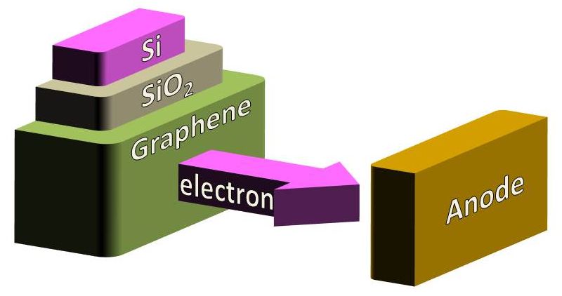 | ||
| K. Nishiguchi, D. Yoshizumi, Y. Sekine, K. Furukawa, A. Fujiwara, and M. Nagase | |||
| [ABSTRACT] We have fabricated a planar cold cathode based on a multilayer (ML)-graphene/SiO2/Si heterostructure. When voltage is applied between the ML graphene and Si layer, electrons tunnel from the Si layer to the ML-graphene through the SiO2. During this tunneling event, electrons repeatedly gain and lose energy in the SiO2 owing to the electric field and scattering, respectively. Electrons whose energy is larger than the work function of the ML-graphene are emitted from its surface to a vacuum. The thinness of the ML-graphene reduces the energy loss of electrons in it and thus improves electron emission characteristics. | |||
| Hopf and period-doubling bifurcations in an electromechanical resonator | |||
| Appl. Phys. Lett. vol. 109, p. 073101 (2016). | |||
| I. Mahboob, R. Dupuy, K. Nishiguchi, A. Fujiwara, and H. Yamaguchi | |||
| [ABSTRACT] An electromechanical resonator is developed in which the dissipation can be dynamically eliminated. The resultant motional dynamics captured by the Van der Pol equation of motion opens up the possibility of a Hopf bifurcation where the mechanical resonance loses stability when the dissipation is eliminated and period-doubling bifurcations when the dissipation becomes negative. In this latter regime, the mechanical spectral response is characterised by multi-stability spanning a bandwidth that is more than an order of magnitude wider than the intrinsic linewidth and it sustains a peak structure that can be tuned by the input used to dynamically manipulate the dissipation. | |||
| An electromechanical displacement transducer | |||
| Appl. Phys. Exp. vol. 9, p. 086701 (2016). | |||
| M. Villiers, I. Mahboob, K. Nishiguchi, D. Hatanaka, A. Fujiwara, and H. Yamaguchi | |||
| [ABSTRACT] Two modes of an electromechanical resonator are coupled through the strain inside the structure with a cooperativity as high as 107, a state-of-the-art value for purely mechanical systems, which enables the observation of normal-mode splitting. This coupling is exploited to transduce the resonator's fundamental mode into the bandwidth of the second flexural mode, which is 1.4 MHz higher in frequency. Thus, an all-mechanical heterodyne detection scheme is implemented that can be developed into a high-precision displacement sensor. | |||
| Fabrication and single-electron-transfer operation of a triple-dot single-electron transistor | |||
| J. Appl. Phys. vol. 118, p. 214305 (2015). | |||
| M. Jo, T. Uchida, A. Tsurumaki-Fukuchi, M. Arita, A. Fujiwara, Y. Ono, K. Nishiguchi, H. Inokawa, and Y. Takahashi | |||
| [ABSTRACT] A triple-dot single-electron transistor was fabricated on silicon-on-insulator wafer using pattern-dependent oxidation. A specially designed one-dimensional silicon wire having small constrictions at both ends was converted to a triple-dot single-electron transistor by means of pattern-dependent oxidation. The fabrication of the center dot involved quantum size effects and stress-induced band gap reduction, whereas that of the two side dots involved thickness modulation because of the complex edge structure of two-dimensional silicon. Single-electron turnstile operation was confirmed at 8 K when a 100-mV, 1-MHz square wave was applied. Monte Carlo simulations indicated that such a device with inhomogeneous tunnel and gate capacitances can exhibit single-electron transfer. | |||
| Thermal-noise suppression in nano-scale Si field-effect transistors by feedback control based on single-electron detection | |||
| Appl. Phys. Lett. vol. 107, p. 073110 (2015). | |||
| K. Chida, K. Nishiguchi, G. Yamahata, H. Tanaka, and A. Fujiwara | |||
| [ABSTRACT] We perform feedback (FB) control for suppressing thermal fluctuation in the number of electrons in a silicon single-electron (SE) device composed of a small transistor and capacitor. SEs enter and leave the capacitor via the transistor randomly at thermal equilibrium, which is monitored in real time using a high-charge-sensitivity detector. In order to suppress such random motion or thermal fluctuation of the electrons, SEs are injected and removed using the transistor according to the monitored change in the number of electrons in the capacitor, which is exactly the FB control. As a result, thermal fluctuation in the number of electrons in a SE device is suppressed by 60%, which corresponds to the so-called FB cooling from 300 to 110 K. Moreover, a thermodynamics analysis of this FB cooling reveals that entropy in the capacitor is reduced and the device is at non equilibrium; i.e., the free energy of the device increases. Since this entropy reduction originates from information about the electrons’ motion monitored by the detector, our results by the FB control represent one type of information-to-energy conversion. | |||
| Observing the semiconducting band-gap alignment of MoS2 layers of different atomic thicknesses using a MoS2/SiO2/Si heterojunction tunnel diode | |||
| Selected for the Featured Article and cover image | |||
| Appl. Phys. Lett. vol. 107, 053101 (2015). | Tunnel diode 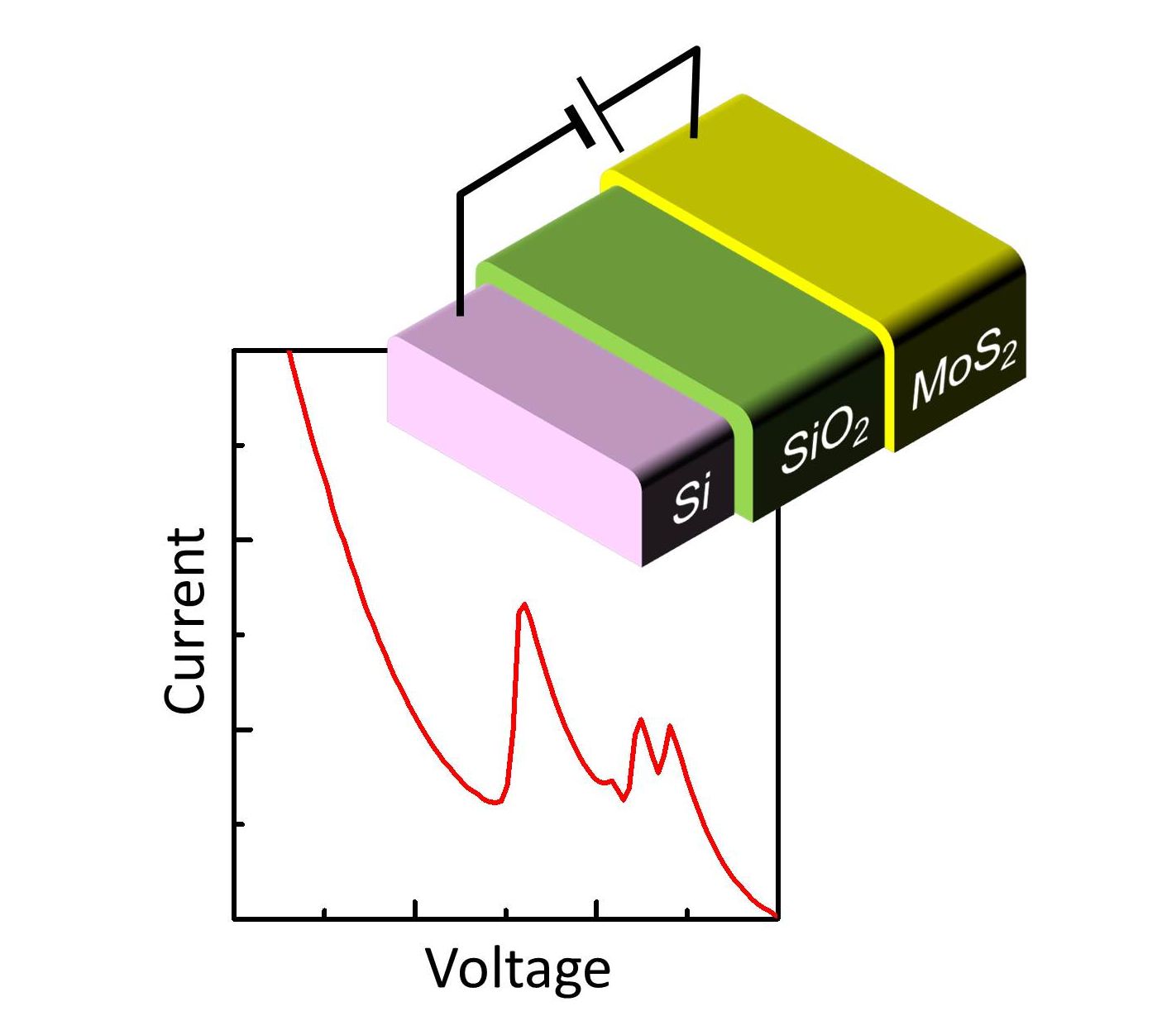 | ||
| K. Nishiguchi, A. Castellanos-Gomez, H. Yamaguchi, A. Fujiwara, H.S. J. van der Zant, G. A. Steele | |||
| [ABSTRACT] We demonstrate a tunnel diode composed of a vertical MoS2/SiO2/Si heterostructure. A MoS2 flake consisting four areas of different thickness functions as a gate terminal of a silicon field-effect transistor. A thin gate oxide allows tunneling current to flow between the n-type MoS2 layers and p-type Si channel. The tunneling-current characteristics show multiple negative differential resistance features, which we interpret as an indication of different conduction-band alignments of the MoS2 layers of different thickness. The presented tunnel device can be also used as a hy-brid-heterostructure device combining the advantages of two-dimensional materials with those of silicon transistors. | |||
| Deviation from the law of energy equipartition in a small dynamic-random-access memory | |||
|
Picked up in Spotlights. | |||
| Jpn. J. Appl. Phys. vol. 54, 06FG03 (2015). | Single-electron detection of thermal noise 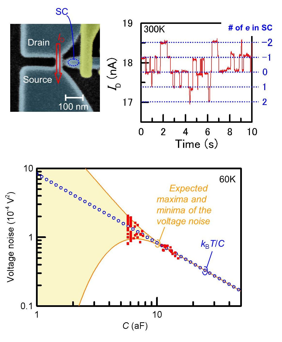 | ||
| P. A. Carles, K. Nishiguchi, and A. Fujiwara | |||
| [ABSTRACT] A small dynamic-random-access memory (DRAM) coupled with a high charge sensitivity electrometer based on a silicon field-effect transistor is used to study the law of equipartition of energy. By statistically analyzing the movement of single electrons in the DRAM at various temperature and voltage conditions in thermal equilibrium, we are able to observe a behavior that differs from what is predicted by the law of equipartition energy: when the charging energy of the capacitor of the DRAM is comparable to or smaller than the thermal energy kBT/2, random electron motion is ruled perfectly by thermal energy; on the other hand, when the charging energy becomes higher in relation to the thermal energy kBT/2, random electron motion is suppressed which indicates a deviation from the law of equipartition of energy. Since the law of equipartition is analyzed using the DRAM, one of the most familiar devices, we believe that our results are perfectly universal among all electronic devices. | |||
| Dispersive and Dissipative Coupling in a Micromechanical Resonator Embedded with a Nanomechanical Resonator | |||
| Nano Letters vol. 15, pp. 2312-2317 (2015). | |||
| I. Mahboob, N. Perrissin , K. Nishiguchi , D. Hatanaka , Y. Okazaki , A. Fujiwara , and H. Yamaguchi | |||
| [ABSTRACT] A micromechanical resonator embedded with a nanomechanical resonator is developed whose dynamics can be captured by the coupled-Van der Pol–Duffing equations. Activating the nanomechanical resonator can dispersively shift the micromechanical resonance by more than 100 times its bandwidth and concurrently increase its energy dissipation rate to the point where it can even be deactivated. The coupled-Van der Pol–Duffing equations also suggest the possibility of self-oscillations. In the limit of strong excitation for the nanomechanical resonator, the dissipation in the micromechanical resonator can not only be reduced, resulting in a quality factor of >3× 10^6, it can even be eliminated entirely resulting in the micromechanical resonator spontaneously vibrating. | |||
| Compact 1D-silicon photonic crystal electro-optic modulator operating with ultra-low switching voltage and energy | |||
| Optics Express vol. 22, pp. 28623-28634 (2014). | |||
| A. Shakoor, K. Nozaki, E. Kuramochi, K. Nishiguchi, A. Shinya, and M. Notomi | |||
| [ABSTRACT] We demonstrate a small foot print (600 nm wide) 1D silicon photonic crystal electro-optic modulator operating with only a 50 mV swing voltage and 0.1 fJ/bit switching energy at GHz speeds, which are the lowest values ever reported for a silicon electro-optic modulator. A 3 dB extinction ratio is demonstrated with an ultra-low 50 mV swing voltage with a total device energy consumption of 42.8 fJ/bit, which is dominated by the state holding energy. The total energy consumption is reduced to 14.65 fJ/bit for a 300 mV swing voltage while still keeping the switching energy at less than 2 fJ/bit. Under optimum voltage conditions, the device operates with a maximum speed of 3 Gbps with 8 dB extinction ratio, which rises to 11 dB for a 1 Gbps modulation speed. | |||
| Electric tuning of direct-indirect optical transitions in silicon | |||
| Sci. Rep. vol. 4, p. 6950 (6 pages) (2014). | |||
| J. Noborisaka, K. Nishiguchi, and A. Fujiwara | |||
| [ABSTRACT] Electronic band structures in semiconductors are uniquely determined by the constituent elements of the lattice. For example, bulk silicon has an indirect bandgap and it prohibits efficient light emission. Here we report the electrical tuning of the direct/indirect band optical transition in an ultrathin silicon-on-insulator (SOI) gated metal-oxide-semiconductor (MOS) light-emitting diode. A special Si/SiO2 interface formed by high-temperature annealing that shows stronger valley coupling enables us to observe phononless direct optical transition. Furthermore, by controlling the gate field, its strength can be electrically tuned to 16 times that of the indirect transition, which is nearly 800 times larger than the weak direct transition in bulk silicon. These results will therefore assist the development of both complementary MOS (CMOS)-compatible silicon photonics and the emerging “valleytronics” based on the control of the valley degree of freedom. | |||
| Gigahertz single-trap electron pumps in silicon | |||
| Nat. Commun. vol. 5, p. 5038 (2014). | |||
| G. Yamahata, K. Nishiguchi, and A. Fujiwara | |||
| [ABSTRACT] Manipulation of single electrons is the key to developing ultimate electronics such as single-electron-based information processors and electrical standards in metrology. Especially, high-frequency and high-accuracy single-electron pumps are essential to realize practical current standards. While electrically defined quantum dots are widely used to build single-electron pumps, a localized state in semiconductors is also a potential candidate for accurate pumps because it can have a large activation energy for the captured electron. However, the transfer mechanism of such localized-state-mediated single-electron pumps for high-accuracy operation at a high frequency has not been well examined. Here we demonstrate a single-electron pump using a single-trap level with an activation energy of a few ten millielectron volts in Si nanotransistors. By means of gate control of capture and emission rates, the pump operates at a frequency of 3 GHz with an accuracy of better than 10^−3 at 17 K, indicating that an electric field at the trap level lowers the capture and emission time to less than 25 ps. | |||
| Single-electron thermal noise | |||
|
Picked up in LAB TALK of nanotechweb.org and Nanotechnology. Picked up in IOPselect. | |||
| Nanotechnology vol. 25, p. 275201 (2014). | Single-electron detection of thermal noise 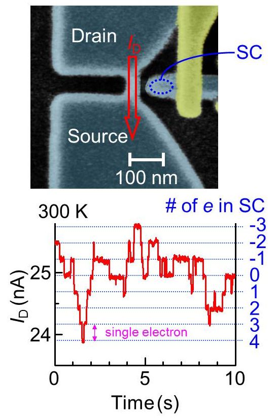 | ||
| K. Nishiguchi, Y. Ono, and A. Fujiwara | |||
| [ABSTRACT] We report the observation of thermal noise on the motion of single electrons in an ultimately small dynamic random access memory (DRAM). Nanometer-scale transistors composing the DRAM resolve the thermal noise in single-electron motion. A complete set of fundamental tests conducted on this single-electron thermal noise shows that this noise perfectly follows all the aspects predicted by the statistical mechanics, which include the occupation probability, the law of equipartition, a detailed balance, and the law of kT/C. In addition, the counting statistics on the directional motion, i.e., the current, of the single-electron thermal noise indicate that the individual electron motion follows the Poisson process like in shot noise. | |||
| Accuracy evaluation and mechanism crossover of single-electron transfer in Si tunable-barrier turnstiles | |||
| Phys. Rev. B, vol. 89, p. 165302 (2014). | |||
| G. Yamahata, K. Nishiguchi, and A. Fujiwara | |||
| [ABSTRACT] Using an error-counting scheme, we evaluated the accuracy of single-electron (SE) transfer in Si tunable-barrier turnstiles in a dilution refrigerator. The error counting was performed by shuttling SEs between a lead and a charge-accumulating node and detecting in real time the number of electrons in the node with an SE-resolution charge sensor. The best experimentally obtained error rate is about 100 parts per million (ppm), where the SE capture in the SE island occurs in thermal equilibrium due to the heating effect on SEs caused by pulse voltages applied to modulate the potential barrier. When we reduce the heating effect by suppressing the pulse voltages, there is a change in the SE transfer mechanism to nonequilibrium SE capture. We theoretically discuss the crossover point of the change. Moreover, at the minimum pulse voltage, the theoretical lower of the error rate estimated by fitting is on the order of 0.01 ppm. This suggests that Si SE-transfer devices are promising candidates for use as quantum current standards in metrology. | |||
| A multimode electromechanical parametric resonator array | |
| Sci. Rep. vol. 4, p. 4448 (2014). | |
| I. Mahboob, M. Mounaix, K. Nishiguchi, A. Fujiwara, and H. Yamaguchi | |
| [ABSTRACT] Electromechanical resonators have emerged as a versatile platform in which detectors with unprecedented sensitivities and quantum mechanics in a macroscopic context can be developed. These schemes invariably utilise a single resonator but increasingly the concept of an array of electromechanical resonators is promising a wealth of new possibilities. In spite of this, experimental realisations of such arrays have remained scarce due to the formidable challenges involved in their fabrication. In a variation to this approach, we identify 75 harmonic vibration modes in a single electromechanical resonator of which 7 can also be parametrically excited. The parametrically resonating modes exhibit vibrations with only 2 oscillation phases which are used to build a binary information array. We exploit this array to execute a mechanical byte memory, a shift-register and a controlled-NOT gate thus vividly illustrating the availability and functionality of an electromechanical resonator array by simply utilising higher order vibration modes. | |
| A simple and inexpensive technique for PDMS/silicon chip alignment with sub-μm precision | |
| Anal. Methods vol.6, p. 97 (2014). | |
| R. Sivakumarasamy, K. Nishiguchi, A. Fujiwara, D. Vuillaume, and N. Clement | |
| [ABSTRACT] This paper describes a novel simple and inexpensive assembly technique with highly accurate alignment of a polydimethylsiloxane (PDMS) layer on a silicon chip for hybrid microfluidic/electronic applications. It is based on strong electrostatic adhesion of a 200 μm thick and dense layer of PDMS onto a metallic cylindrical tool mechanically fixed to an optical microscope. A 2 mm hole in the tool allows precise alignment of the PDMS layer, 10 μm from the surface, without the usage of any lubricant. The same tool is used for PDMS bonding in a well-controlled manner. This technique is compatible with wafer scale alignment. A very precise consideration of the PDMS shrinkage ratio, reduced by 50% for thin layers, enables a misalignment range of less than 1 μm in the experiments. | |
| Multi-mode parametric coupling in an electromechanical resonator | |
| Appl. Phys. Lett. vol. 103, p. 153105 (2013). | |
| I. Mahboob, V. Nier, K. Nishiguchi, A. Fujiwara, and H. Yamaguchi | |
| [ABSTRACT] Parametric coupling between multiple vibration modes in an electromechanical resonator is demonstrated via a strain inducing piezoelectric pump which enables construction of a mechanical-vibration register. In particular, the coupling between the flexural and torsional vibration modes can exceed their intrinsic dissipation rates enabling operation deep into the strong-coupling regime. The dynamic nature of this parametric coupling also permits temporal manipulation of the mechanical-vibration register enabling both long-lived modes to be rapidly switched off and phonon populations to be coherently exchanged between modes. | |
| Wide-bandwidth charge sensitivity with a radio-frequency field-effect transistor | |||
| Appl. Phys. Lett. vol. 103, p. 143102 (2013). | Fast charge sensing using an FET combined with an LC circuit 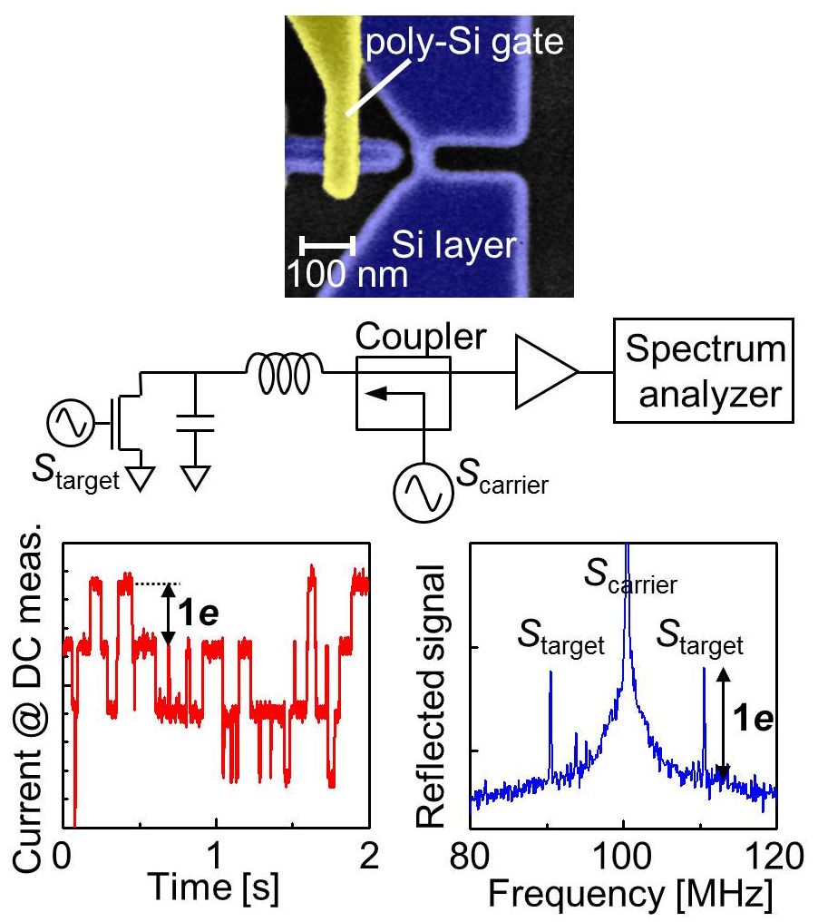 | ||
| K. Nishiguchi, H. Yamaguchi, A. Fujiwara, H. S. J. Zant, and G. A. Steele | |||
| [ABSTRACT] We demonstrate high-speed charge detection at room temperature with single-electron resolution by using a radio-frequency field-effect transistor (RF-FET). The RF-FET combines a nanometer-scale silicon FET with an impedance-matching circuit composed of an inductor and capacitor. Driving the RF-FET with a carrier signal at resonance frequency, small signals at the transistor’s gate modulate the resonance condition, which is monitored at high speed using the reflected signal. The RF-FET driven by high-power carrier signals enables a charge sensitivity of 2×10^-4 e/Hz^0.5 at readout band-width of 20 MHz. | |||
| Water Electrolysis and Energy Harvesting with Zero-Dimensional Ion-Sensitive Field-Effect Transistors | |
| Nano Lett. vol. 13, p. 3903 (2013) | |
| N. Clément, K. Nishiguchi, J. F. Dufreche, D. Guerin, A. Fujiwara, and D. Vuillaume | |
| [ABSTRACT]The relationship of the gas bubble size to the size distribution critically influences the effectiveness of electrochemical processes. Several optical and acoustical techniques have been used to characterize the size and emission frequency of bubbles. Here, we used zero-dimensional (0D) ion-sensitive field-effect transistors (ISFETs) buried under a microbath to detect the emission of individual bubbles electrically and to generate statistics on the bubble emission time. The bubble size was evaluated via a simple model of the electrolytic current. We suggest that energy lost during water electrolysis could be used to generate electric pulses at an optimal efficiency with an array of 0D ISFETs. | |
| Phonon Lasing in an Electromechanical Resonator | |
| Phys. Rev. Lett. vol. 110, p. 127202 (2013) | |
| I. Mahboob, K. Nishiguchi, A. Fujiwara, and H. Yamaguchi | |
| [ABSTRACT]An electromechanical resonator harboring an atomlike spectrum of discrete mechanical vibrations, namely, phonon modes, has been developed. A purely mechanical three-mode system becomes available in the electromechanical atom in which the energy difference of the two higher modes is resonant with a long-lived lower mode. Our measurements reveal that even an incoherent input into the higher mode results in coherent emission in the lower mode that exhibits all the hallmarks of phonon lasing in a process that is reminiscent of Brillouin lasing. | |
| Detecting signals buried in noise via nanowire transistors using stochastic resonance | |||
| Appl. Phys. Lett. vol. 101, p. 193108 (2012). | Signal detection using a transitor with small S-swing  | ||
| K. Nishiguchi and A. Fujiwara | |||
| [ABSTRACT] We demonstrate stochastic resonance (SR), which takes advantage of noise to detect a weak signal, using a field-effect transistor (FET). An FET’s structure composed of a nanowire channel enables current characteristics to show strong nonlinearity, which overcomes thermal limitation, and dynamic bistability, both of which boost an effect of SR and silhouette noise from noise. Moreover, the dynamic bistability enables SR effect to be enhanced by adding common noise to multiple FETs. The FET providing such unique characteristics opens the way to use SR for practical applications. | |||
| Nanowire Metal-Oxide-Semiconductor Field-Effect Transistors with Small Subthreshold | |||
| Appl. Phys. Express, vol. 5, p. 085002 (2012). | Transitor with small S-swing | ||
| K. Nishiguchi and A. Fujiwara | |||
| [ABSTRACT]We demonstrate metal-oxide-semiconductor field-effect transistors (MOSFETs) with small subthreshold swing (SS). The MOSFETs have a nanowire channel and three gates. A parasitic bipolar transistor formed in a fully depleted silicon-on-insulator MOSFET applies body bias to the MOSFET’s channel and thus reduces the SS. Additionally, triple-gate operation makes drain voltage smaller and provides current characteristics with a high on/off ratio and small hysteresis. As a result, SSs of the n-type and p-type MOSFETs reach 6.6 and 5.2 mV/dec, respectively, in the range of current of six orders of magnitude. These features promise MOSFETs with low power consumption. | |||
| Phonon-cavity electromechanics | |
| Nature Physics, vol. 8, pp. 387-392 (2012) | |
| I. Mahboob, K. Nishiguchi, H. Okamoto, and H. Yamaguchi | |
| [ABSTRACT]Photonic cavities have emerged as an indispensable tool to control and manipulate harmonic motion in opto/electromechanical systems. Invariably, in these systems a high-quality-factor photonic mode is parametrically coupled to a high-quality-factor mechanical oscillation mode. This entails the demanding challenges of either combining two physically distinct systems, or else optimizing the same nanostructure for both mechanical and optical properties. In contrast to these approaches, here we show that the cavity can be realized by the second oscillation mode of the same mechanical oscillator. A piezoelectric pump generates strain-induced parametric coupling between the first and the second mode at a rate that can exceed their intrinsic relaxation rate. This leads to a mechanically induced transparency in the second mode which plays the role of the phonon cavity, the emergence of parametric normal-mode splittingand the ability to cool the first mode. Thus, the mechanical oscillator can now be completely manipulated by a phonon cavity | |
| Tuneable electromechanical comb generation | |
| Appl. Phys. Lett. vol. 100, p. 113109 (2012) | |
| I. Mahboob, Q. Wilmart, K. Nishiguchi, A. Fujiwara, and H. Yamaguchi | |
| [ABSTRACT]An array of equally spaced oscillations or a comb is created within the bandwidth of the fundamental mode of an electromechanical resonator. This phenomenon utilises 2 continuous-wave (CW) pump excitations that piezoelectrically modulate the tension in the mechanical element and is seeded by a CW harmonic excitation of the first mode i.e., the signal. The resultant comb can be dynamically manipulated via the pumps and signal where the teeth separation can be tuned over 3 orders of magnitude and the comb density can be increased from just 2 teeth to nearly 10^2. (c) 2012 American Institute of Physics | |
| Bound exciton photoluminescence from ion-implanted phosphorus in thin silicon layers | |
| Optics Express, vol. 19, p. 25255 (2011). | |
| H. Sumikura, K. Nishiguchi, Y. Ono, A. Fujiwara, and M. Notomi | |
| [ABSTRACT]We report the observation of clear bound exciton (BE) emission from ion-implanted phosphorus. Shallow implantation and high-temperature annealing successfully introduce active donors into thin silicon layers. The BE emission at a wavelength of 1079 nm shows that a part of the implanted donors are definitely activated and isolated from each other. However, photoluminescence and electron spin resonance studies find a cluster state of the activated donors. The BE emission is suppressed by this cluster state rather than the nonradiative processes caused by ion implantation. Our results provide important information about ion implantation for doping quantum devices with phosphorus quantum bits. (c) 2011 OSA | |
| Wide-band idler generation in a GaAs electromechanical resonator | |
| Phys. Rev. B, vol. 84, p. 113411 (2011). | |
| I. Mahboob, Q. Wilmart, K. Nishiguchi, A. Fujiwara, and H. Yamaguchi | |
| [ABSTRACT]Periodically modulating the piezoelectrically introduced strain in an electromechanical resonator can enable the fundamental (ω0) and the first modes (ω1) to be coupled. This is explicitly demonstrated with the creation of a mechanical idler at ω1 (ω0) when a signal excitation is applied at ω0 (ω1) and a pump excitation is applied at ω0+ω1. The dynamics of the mechanical idler generation are captured by a simple phenomenological model and our experimental demonstration paves the way toward accessing the diverse functionality of nonlinear optics in an on-chip electromechanical platform. | |
| Evaluation of a Gate Capacitance in the Sub-aF Range for a Chemical Field-Effect Transistor With a Si Nanowire Channel | |
| IEEE Trans. Nanotechnology, vol. 10, p. 1172 (2011). | |
| N. Clement, K. Nishiguchi, A. Fujiwara, and D. Vuillaume | |
| [ABSTRACT]An evaluation of the gate capacitance of a field-effect transitor (FET), whose channel length and width are several ten nanometer, is a key point for sensors applications. However, experimental and precise evaluation of capacitance in the attofarad range or less has been extremely difficult. Here, we report an extraction of the capacitance down to 0.55 aF for a Si FET with a nanoscale wire channel, whose width and length are 15 and 50 nm, respectively. The extraction can be achieved by using a combination of four kinds of measurements: current characteristics modulated by double gates, random-telegraph-signal noise induced by trapping and detrapping of a single electron, dielectric polarization noise, and current characteristics showing Coulomb blockade at low temperature. The extraction of such a small gate capacitance enables us to evaluate electron mobility in a nanoscale wire by using a classical model of current characteristics of an FET. | |
| Large Array of Sub-10-nm Single-Grain Au Nanodots for use in Nanotechnology | |
| Small, V. 7, pp. 2607-2613 (2011). | |
| N. Clement, G. Patriarche, K. Smaali, F. Vaurette, K. Nishiguchi, D. Troadec, A. Fujiwara, and D. Vuillaume | |
| [ABSTRACT]A uniform array of single-grain Au nanodots, as small as 5--8 nm, can be formed on silicon using e-beam lithography. The as-fabricated nanodots are amorphous, and thermal annealing converts them to pure Au single crystals covered with a thin SiO2 layer. These findings are based on physical measurements, such as atomic force microscopy (AFM), atomic-resolution scanning transmission electron microscopy, and chemical techniques using energy dispersive X-ray spectroscopy. A self-assembled organic monolayer is grafted on the nanodots and characterized chemically with nanometric lateral resolution. The extended uniform array of nanodots is used as a new test-bed for molecular electronic devices. | |
| Single-Electron Stochastic Resonance Using Si Nanowire Transistors | |||
| Picked up in SPOTLIGHTS: Editors'Choice from APEX and JJAP. | |||
| Jpn. J. Appl. Phys., vol. 50, p. 06GF04 (2011). | Patern perception using stochastic resonace  |
||
| K. Nishiguchi and A. Fujiwara | |||
| [ABSTRACT] We demonstrate stochastic resonance (SR) with single electrons (SEs) using nanoscale metal-oxide-semiconductor field-effect transistors (MOSFETs). Input signal applied to a MOSFET modulates SE transport in an average manner based on nonlinear characteristics. On the other hand, an individual SE goes through the MOSFET in a completely random manner, which corresponds to shot noise. SEs transferred to a storage node are counted precisely by the other MOSFET and used as an output signal. The correlation between the input and output signals is improved by taking advantage of extrinsic noise as well as the intrinsic shot noise composed of SEs. It is confirmed that the shot-noise-assisted SR allows fast operation with a simple system. Pattern perception utilizing SR is also demonstrated. | |||
| Single-electron counting statistics of shot noise in nanowire Si metal-oxide-semiconductor field-effect transistors | |||
| Picked up in the May 23, 20011 issue of Virtual Journal of Nanoscale Science & Technology | |||
| Appl. Phys. Lett., vol. 98, p. 193502 (2011). | Time-domain analysis on shot noise 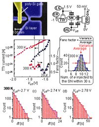 | ||
| K. Nishiguchi, Y. Ono, and A. Fujiwara | |||
| [ABSTRACT] Shot noise in the transport of single electrons in a Si metal-oxide-semiconductor field-effect transistor is monitored by real-time measurement with a high-charge-sensitivity electrometer. In the current range between zepto and attoamperes, the current characteristics are found to be divided into two regimes: a temperature-independent regime in the lower current range and a temperature-dependent one in the higher current range. A time-domain analysis reveals that, for both regimes, the single-electron transport obeys a pure Poisson process with the Fano factor’s being nearly unity, while the shot noise is suppressed with reduced Fano factors around the boundary. c 2011 American Institute of Physics | |||
| Accuracy evaluation of single-electron shuttle transfer in Si nanowire metal-oxide-semiconductor field-effect transistors | |
| Appl. Phys. Lett., vol. 98, p. 222104 (2011). | |
| G. Yamahata, K. Nishiguchi, and A. Fujiwara | |
| [ABSTRACT] We report on evaluation of transfer accuracy in a single-electron turnstile using silicon nanowire metal-oxide-semiconductor field-effect transistors at 17 K. Single-electron shuttle transfer and single-shot detection of a single electron are used to detect errors of the transfer. Errors for the transfer through an electrostatically formed island are ascribed to thermal processes. We also observed single-electron transfer mediated by a trap level, which exhibits a wide current plateau and a low error rate. c 2011 American Institute of Physics | |
| Strong Stark effect in electroluminescence from phosphorous-doped silicon-on-insulator metal-oxide-semiconductor field-effect transistors | |||
| Appl. Phys. Lett., vol. 98, p. 033503 (2011). | |||
| J. Noborisaka, K. Nishiguchi, Y. Ono, H. Kageshima, and A. Fujiwara | |||
| [ABSTRACT] We report a strong Stark effect in electroluminescence (EL) from thin silicon-on-insulator metal-oxide-semiconductor field-effect transistors. The EL peak shows a large Stark shift of up to 50 meV when a gate-induced electric field is applied. Such a large shift is observed because of the strong confinement of carriers by a Si/SiO2 quantum well. Furthermore, we observe a sudden decrease of EL intensity at a specific electric field. This feature is ascribed to electron dissociation from phosphorous atom to subbands in a triangular well at the Si/SiO2 interface by the applied electric field. c 2011 American Institute of Physics | |||
| Interconnect-free parallel logic circuits in a single mechanical resonator | |||
| Nature Communications, v. 2, p. 198 (2011). | |||
| I. Mahboob, E. Flurin, K. Nishiguchi, A. Fujiwara, and H. Yamaguchi | |||
| [ABSTRACT] In conventional computers, wiring between transistors is required to enable the execution of Boolean logic functions. This has resulted in processors in which billions of transistors are physically interconnected, which limits integration densities, gives rise to huge power consumption and restricts processing speeds. A method to eliminate wiring amongst transistors by condensing Boolean logic into a single active element is thus highly desirable. Here, we demonstrate a novel logic architecture using only a single electromechanical parametric resonator into which multiple channels of binary information are encoded as mechanical oscillations at different frequencies. The parametric resonator can mix these channels, resulting in new mechanical oscillation states that enable the construction of AND, OR and XOR logic gates as well as multibit logic circuits. Moreover, the mechanical logic gates and circuits can be executed simultaneously, giving rise to the prospect of a parallel logic processor in just a single mechanical resonator. | |||
| A silicon nanowire ion-sensitive field-effect transistor with elementary charge sensitivity | |||
| Appl. Phys. Lett., vol. 98, p. 014104 (2011). | |||
| N. Clement, K. Nishiguchi, J. F. Dufreche, D. Guerin, A. Fujiwara, and D. Vuillaume | |||
| [ABSTRACT] We investigate the mechanisms responsible for the low-frequency noise in liquid-gated nanoscale silicon nanowire field-effect transistors (SiNW-FETs) and show that the charge-noise level is lower than elementary charge. Our measurements also show that ionic strength of the surrounding electrolyte has a minimal effect on the overall noise. Dielectric polarization noise seems to be at the origin of the 1/f noise in our devices. The estimated spectral density of charge noise Sq = 1.6×10^-2 e/Hz^1/2 at 10 Hz opens the door to metrological studies with these SiNW-FETs for the electrical detection of a small number of molecules. c 2011 American Institute of Physics | |||
| Enhanced force sensitivity and noise squeezing in an electromechanical resonator coupled to a nanotransistor | |||
| Appl. Phys. Lett., vol. 97, p. 253105 (2010). | |||
| I. Mahboob, E. Flurin, K. Nishiguchi, A. Fujiwara, and H. Yamaguchi | |||
| [ABSTRACT] A nanofield-effect transistor (nano-FET) is coupled to a massive piezoelectricity based electromechanical resonator integrated with a parametric amplifier. The mechanical parametric amplifier can enhance the resonator’s displacement and the resulting electrical signal is further amplified by the nano-FET. This hybrid amplification scheme yields an increase in the mechanical displacement signal by 70 dB resulting in a force sensitivity of 200 aNHz^-1/2 at 3 K. The mechanical parametric amplifier can also squeeze the displacement noise in one oscillation phase by 5 dB enabling a factor of 4 reduction in the thermomechanical noise force level. c 2010 American Institute of Physics | |||
| Separately contacted monocrystalline silicon double-layer structure with an amorphous silicon dioxide barrier made by wafer bonding | |||
| Semiconductor Science and Technology, vol. 25, p. 125001 (2010) | |||
| K. Takashina, M. Nagase, K. Nishiguchi, Y. Ono, H. Omi, A. Fujiwara, T. Fujisawa, and K. Muraki | |||
| [ABSTRACT] A double layer of monocrystalline silicon separated by a 23.5 nm silicon dioxide barrier is fabricated by bonding two silicon-on-insulator wafers with oxidized surface layers. The two layers are separately contacted allowing transport measurements through individual layers and a bias voltage to be applied between the layers. Four-terminal magnetotransport measurements at cryogenic temperatures on electrons generated close to the central oxide barrier show reasonable mobility. | |||
| One-by-one trap activation in silicon nanowire transistors | |||
| Nature Communications, v. 1, p. 92 (2010). | |||
| N. Clement , K. Nishiguchi, A. Fujiwara, and D. Vuillaume | |||
| [ABSTRACT] Flicker or 1/f noise in metal-oxide-semiconductor field-effect transistors (MOSFETs) has been identified as the main source of noise at low frequency. It often originates from an ensemble of a huge number of charges becoming trapped and de-trapped. However, as a deviation from the well-known model of 1/f noise is observed for nanoscale MOSFETs, a new model is required. Here, we report the observation of one-by-one trap activation controlled by the gate voltage in a nanowire MOSFET and propose a new low-frequency-noise theory for nanoscale FETs. We show that the Coulomb repulsion between electronically charged trap sites prevents the activation of several traps simultaneously. This effect induces a noise reduction of more than one order of magnitude. It decreases when the electron density in the channel is increased due to the electrical screening of traps. These findings are technologically useful for any FET with a short and narrow channel. | |||
| Resonant escape over an oscillating barrier in a single-electron ratchet transfer | |||
| Phys. Rev. B, vol. 82, p. 033303 (2010). | |||
| S. Miyamoto, K. Nishiguchi, Y. Ono, K. M. Itoh, and A. Fujiwara | |||
| [ABSTRACT] Single-electron escape from a metastable state over an oscillating barrier is experimentally investigated in silicon-based ratchet transfer. When the barrier is oscillating on a time-scale characteristic of the single-electron escape, synchronization occurs between the deterministic barrier modulation and the stochastic escape events. The average escape time as a function of its oscillation frequency exhibits a minimum providing a primary signature for resonant activation of single electrons. c 2010 The American Physical Society | |||
| Tunneling spectroscopy of electron subbands in thin silicon-on-insulator metal-oxide-semiconductor field-effect transistors | |||
| Appl. Phys. Lett., vol. 96, p. 112102 (2010). | |||
| J. Noborisaka, K. Nishiguchi, H. Kageshima, Y. Ono, and A. Fujiwara | |||
| [ABSTRACT] We report the tunneling spectroscopy of thin silicon-on-insulator (SOI) metal-oxide-semiconductor field-effect transistors with tunneling gate oxide. When electrons are injected into a thin SOI well, the gate-tunneling current shows kink structures originating from quantized energy levels in the SOI well. From the theoretical consideration of the energy levels and their density of states, the observed features can be ascribed to electron tunneling into the in-plane fourfold degenerate valley subbands. Furthermore, inhomogeneous peak broadening of the kink structures in the experiment is well explained by the SOI thickness variation. c 2010 American Institute of Physics | |||
| Si nanowire ion-sensitive field-effect transistors with a shared floating gate | |||
| Appl. Phys. Lett., vol. 94, p. 163106 (2009). | Real-time monitoring of molecules  | ||
| K. Nishiguchi, N. Clement , T. Yamaguchi, and A. Fujiwara | |||
| [ABSTRACT] Ion-sensitive field-effect transistors (ISFETs) arrayed in parallel were fabricated on a silicon-on-insulator substrate. Since the nanoscale wire channels of the ISFETs are bridged with a floating gate on which molecules are preferably immobilized, signals originating from charged materials only on the floating gate can appear and can therefore be distinguished from background noise, which leads to noise-robust sensing. Additionally, the nanoscale channels provide the ISFETs with single-electron-resolution charge sensitivity as well as a reduction in background noise induced in the wider channels used as electrical leads. These features promise the detection of a small number of molecules. c 2009 American Institute of Physics | |||
| Single-electron counting statistics and its circuit application in nanoscale field-effect transistors at room temperature | |||
| Nanotechnology, vol. 20, p. 175201 (2009). | Flexible pattern recognition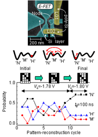 | ||
| K. Nishiguchi and A. Fujiwara | |||
| [ABSTRACT] A circuit utilizing single electrons is demonstrated at room temperature. Individual electrons randomly passing through the nanoscale silicon-on-insulator metal-oxide-semiconductor field-effect transistor (MOSFET) are monitored by an electrometer in real time. Such a random behavior of single electrons is used for high-quality random-number generation suitable for data processing which stochastically extracts the most preferable pattern among various ones. MOSFET-based random-number generation allows fast operation as well as high controllability, which leads to flexible extraction of the preferable pattern. | |||
| Room temperature piezoelectric displacement detection via a silicon field effect transistor | |||
| Appl. Phys. Lett., vol. 95, p. 233102 (2009). | |||
| I. Mahboob, K. Nishiguchi, A. Fujiwara, and H. Yamaguchi | |||
| [ABSTRACT] An electromechanical oscillator embedded with a two dimensional electron gas is capacitively coupled to a silicon field effect transistor (Si-FET). The piezovoltage induced by the mechanical motion modulates the current passing through the Si-FET enabling the electromechanical oscillator’s position to be monitored. When the Si-FET is biased at its optimal point, the motion induced piezovoltage can be amplified resulting in a displacement sensitivity of 6×10^-12mHz-1/2 for a 131 kHz GaAs resonator which is among the highest recorded for an all-electrical room temperature detection scheme. c 2009 American Institute of Physics | |||
| Low power and fast electro-optic silicon modulator with lateral p-i-n embedded photonic crystal nanocavity | |||
| Optics Express, vol. 17, 22505-22513 (2009) | |||
| T. Tanabe, K. Nishiguchi, E. Kuramochi, and M. Notomi | |||
| [ABSTRACT] We have fabricated high-Q photonic crystal nanocavities with a lateral p-i-n structure to demonstrate low-power and high-speed electro-optic modulation in a silicon chip. GHz operation is demonstrated at a very low (μW level) operating power, which is about 4.6 times lower than that reported for other cavities in silicon. This low-power operation is due to the small size and high-Q of the photonic crystal nanocavity. c 2009 OSA | |||
| Horizontal position analysis of single acceptors in Si nanoscale field-effect transistors | |||
| Appl. Phys. Lett., vol. 94, 223501 (2009) | |||
| M. A. H. Khalafalla, Y. Ono, K. Nishiguchi, and A. Fujiwara | |||
| [ABSTRACT] The authors performed conductance measurements to identify the horizontal position of single boron acceptors in silicon-on-insulator nanoscale field-effect transistors at a temperature of 6 K. The horizontal position, i.e., how far the acceptor is from the source or drain terminal, is qualitatively obtained, and it is shown, on the level of single dopants, that the acceptor near the source significantly affects the subthreshold nature of the transistor. c 2009 American Institute of Physics | |||
| Electrons and holes in a 40 nm thick silicon slab at cryogenic temperatures | |||
| Appl. Phys. Lett., vol. 94, 142104 (2009) | |||
| K. Takashina, K. Nishiguchi, Y. Ono, A. Fujiwara, T. Fujisawa, Y. Hirayama, and K. Muraki | |||
| [ABSTRACT] We demonstrate low temperature operation of an electron-hole bilayer device based on a 40 nm thick layer of silicon in which electrons and holes can be simultaneously induced and contacted independently. The device allows the application of bias between the electrons and holes enhancing controllability over density and confining potential. We confirm that drag measurements are possible with the structure. c 2009 American Institute of Physics | |||
| Single-Electron-Resolution Electrometer Based on Field-Effect Transistor | |||
| Picked up in the December 15, 2008 issue of Virtual Journal of Nanoscale Science & Technology | |||
| Jpn. J. Appl. Phys., vol. 47, pp. 8305-8310 (2008). | Single-electron detection at room temperature 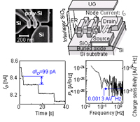 | ||
| K. Nishiguchi, C. Koechlin, Y. Ono, A. Fujiwara, H. Inokawa, and H. Yamaguchi | |||
| [ABSTRACT] An electrometer based on field-effect transistors (FETs) was fabricated on a silicon-on-insulator substrate (SOI). The electrometer has a nanometer-scale small channel and a capacitively coupled node, where single electrons are stored. We discuss the dependence of the charge sensitivity of the electrometer on its structure and on its operation condition and gives guides for achieving the higher charge sensitivity. The device optimization based on this dependence allows the demonstration of the electrometer with extremely high charge sensitivity, 0.0013 e/√Hz at 1 Hz, at room temperature. | |||
| Low-energy electron emission from an electron inversion layer of a Si/SiO2/Si cathode for nano-decomposition | |||
| Jpn. J. Appl. Phys., vol. 47, pp. 5106-5108 (2008). | Electron emission from mos structure 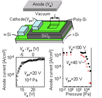 | ||
| K. Nishiguchi, M. Nagase, T. Yamaguchi, A. Fujiwara, and H. Yamaguchi | |||
| [ABSTRACT] We fabricated an electron-emission cathode with a Si/SiO2/Si structure using metal{xide《emiconductor field-effect transistor (MOSFET) fabrication technology. Electrons travel from an electron-source Si layer to a thin polycrystalline Si (poly-Si) through a thin SiO2 and some of them with high energy, i.e., hot electrons, are emitted from the poly-Si surface. By utilizing an electron-inversion layer as the electron source, high efficiency and stability of electron emission were achieved. Material decomposition at a depth of a few nanometers was also demonstrated using a low-energy-electron irradiation from the cathode operated in a low vacuum condition. | |||
| Stochastic data processing circuit based on single electrons using nanoscale field-effect transistors | |||
| Picked up in the February 25, 2008 issue of Virtual Journal
of Nanoscale Science & Technology. Picked up in News and Views of the May 8, 2008 online issue of Nature. | |||
| Appl. Phys. Lett., vol. 92, p. 062105 (2008). | Flexible logic circuit | ||
| K. Nishiguchi, Y. Ono, A. Fujiwara, H. Inokawa, and Y. Takahashi | |||
| [ABSTRACT] A circuit utilizing single electrons is demonstrated at room temperature using a silicon-on-insulator metal-oxide-semiconductor field-effect transistor (MOSFET). Individual electrons randomly passing through the nanoscale MOSFET, which are the origin of shot noise, are monitored by an electrometer in real time. This random behavior of single electrons is used as a random number for a stochastic associative memory for image-pattern matching, in which the most preferable pattern is extracted with the largest probability. The use of electron transport in the MOSFET provides high controllability of the randomness as well as fast generation of random numbers. The present result promises single-electron applications using nanoscale MOSFETs. c 2008 American Institute of Physics | |||
| Charge transport in boron-doped nano MOSFETs: Towards single-dopant electronics | |||
| Appl. Surf. Sci., vol. 254, pp. 6252-6256(2008) | |||
| Y. Ono, M. Khalafalla, K. Nishiguchi, K. Takashina, A. Fujiwara, S. Horiguchi, H. Inokawa, and Y. Takahashi | |||
| [ABSTRACT] We investigate the hole transport in p-channel field-effect transistors doped with boron, at low temperatures (6 - 28 K). In transistors with a relatively large dimension, we observe the acceptor-mediated hopping and carrier freezeout, both of which are strongly influenced by the gate bias. In nanoscale transistors, these features turn into single-charge tunneling, i.e., the trapping/detrapping of single holes by/from individual acceptors. The statistics of the appearance of the modulation in a few ten samples indicates that the number of acceptors is small, or even just one, indicating that what we have observed is single-charge-transistor operation by a single-acceptor quantum dot. (C) 2008 Elsevier B. V. All rights reserved. | |||
| Escape dynamics of a few electrons in a single-electron ratchet using silicon nanowire metal-oxide-semiconductor field-effect transistor | |||
| Appl. Phys. Lett., vol. 93, 222103 (2008) | |||
| S. Miyamoto, K. Nishiguchi, Y. Ono, K M. Itoh, and A. Fujiwara. | |||
| [ABSTRACT] Transport dynamics of a few electrons in a quantum dot are investigated in a single-electron ratchet using silicon nanowire metal-oxide-semiconductor field-effect transistors. Time-resolved measurements in a nanosecond regime are carried out to determine the escape times of the first, second, and third electrons from the quantum dot originally containing three electrons. The escape time strongly depends on the number of electrons due to the single-electron charging effect in the quantum dot, which makes it possible to achieve selective ejection of a desired number of electrons. c 2008 American Institute of Physics | |||
| Silicon single-charge transfer devices | |||
| J. Phys. Chem. Solids Vol. 69, No. 2-3, 702-707 (2008) | |||
| Y. Ono, A. Fujiwara, K. Nishiguchi, Y. Takahashi, and H. Inokawa. | |||
| [ABSTRACT] The single-electron device (SED) enables the control of electron motion on the level of an elementary charge. Single-charge transfer devices are special SEDs that enable single-electron transfer synchronized with the gate clock. They have the potential for extremely low transfer error rates and are expected to be building blocks for future information processing and electrical metrology. We have been pursuing the fabrication of Si-based SEDs using CMOS technology with the help of electron-beam lithography and have recently demonstrated the single-charge transfer devices. The devices are composed of one Si quantum dot sandwitched between two tiny MOS gates and can operate at much higher temperatures than those of former metal-based and compound-semiconductor-based devices. This opens up the possibility of the practical use of clocked single-charge transfer. | |||
| Nanoampere charge pump by single-electron ratchet using silicon nanowire metal-oxide-semiconductor field-effect transistor | |||
| Appl. Phys. Lett., vol. 92, 042102 (2008) | |||
| A. Fujiwara, K. Nishiguchi, and Y. Ono. | |||
| [ABSTRACT] Nanoampere single-electron pumping is presented at 20 K using a single-electron ratchet comprising silicon nanowire metal-oxide-semiconductor field-effect transistors. The ratchet features an asymmetric potential with a pocket that captures single electrons from the source and ejects them to the drain. Directional single-electron transfer is achieved by applying one ac signal with the frequency up to 2.3 GHz. We find anomalous shapes of current steps which can be ascribed to nonadiabatic electron capture. c 2008 American Institute of Physics | |||
| Infrared detection with silicon nano field-effect transistors | |||
| Picked up in the June 11, 2007 issue of Virtual Journal
of Nanoscale Science and Technology Picked up in the August, 2007 issue of Photonics Spectra Picked up in the July, 2007 issue of Laser Focus World | |||
| Appl. Phys. Lett., vol. 90, p. 223108 (2007). | Infrared detection |
||
| K. Nishiguchi, A. Fujiwara, Y. Ono, H. Inokawa, and Y. Takahashi | |||
| [ABSTRACT] The authors fabricated nanoscale silicon metal-oxide-semiconductor field-effect transistors (MOSFETs) to detect an infrared (IR) signal at room temperature. The IR signal excites conduction-band electrons in an undoped channel of a MOSFET and some of them are injected through an energy barrier into a storage node (SN) electrically formed by the MOSFET. Small signals, originating from electrons, stored in the SN are detected by an electrometer with a single-electron resolution. Additionally, the MOSFET controls the number and energy of electrons injected into the SN. This enables electrical control of the sensitivity and cutoff wavelengths of IR signals, suggesting the possibility of highly functional IR sensors. c 2007 American Institute of Physics | |||
| Long retention of gain-cell dynamic random-access memory with undoped memory node | |||
| IEEE Electron Device Lett. vol. 28, pp. 48-50 (2007). | Memory operation with long retention  |
||
| K. Nishiguchi, A. Fujiwara, Y. Ono, H. Inokawa, and Y. Takahashi | |||
| [ABSTRACT] Low current leakage characteristics of a novel silicon-on-insulator (SOI) device are investigated in view of application to a gain-cell dynamic random access memory (DRAM). The device consists of a two-layered poly-Si gate. Since, in this device, the memory node is electrically formed by the gate in undoped SOI wire, no p-n junction is required. The retention is found to be dominated by the subthreshold leakage, which leads to long data retention. The device also achieved a fast (10 ns) writing time and its fabrication process is compatible with those of SOI MOSFETs. The present results, thus, strongly suggest a way of conducting a gain-cell DRAM to be embedded into logic circuits. | |||
| Identification of single and coupled acceptors in silicon nano-field-effect transistors | |||
| Appl. Phys. Lett., vol. 12, 263513 (2007) | |||
| M. A. H. Khalafalla, Y. Ono, K. Nishiguchi, and A. Fujiwara. | |||
| [ABSTRACT] We performed dopant mediated hole transport measurements to identify the depth position of individual boron acceptors and investigate two-acceptor coupling in silicon-on-insulator nanoscale field-effect transistors at a temperature of 6 K. The depth position is qualitatively obtained from the analysis of the acceptor-to-gate capacitances. We also observe signatures of a two-acceptor capacitive coupling in the characteristics of the conductance versus the front and back gate voltages. c 2007 American Institute of Physics | |||
| Transfer and detection of single electrons using metal-oxide-semiconductor field-effect transistors | |||
| IEICE Trans. Electron., vol. E90-C, p. 943 (2007). | |||
| W. Zhang, K. Nishiguchi, Y. Ono, A. Fujiwara, H. Yamaguchi, H. Inokawa, Y. Takahashi, and N. J. Wu. | |||
| [ABSTRACT] A single-electron turnstile and electrometer circuit was fabricated on a silicon-on-insulator substrate. The turnstile, which is operated by opening and closing two metal-oxide-semiconductor field-effect transistors (MOSFETs) alternately, allows current quantization at 20 K due to single-electron transfer. Another MOSFET is placed at the drain side of the turnstile to form an electron storage island. Therefore, one-by-one electron entrance into the storage island from the turnstile can be detected as an abrupt change in the current of the electrometer, which is placed near the storage island and electrically coupled to it. The correspondence between the quantized current and the single-electron counting was confirmed. | |||
| Conductance modulation by individual acceptors in Si nanoscale field-effect transistors | |||
| Appl. Phys. Lett., vol. 90, 102106 (2007). | |||
| Y. Ono, K. Nishiguchi, A. Fujiwara, H. Yamaguchi, H. Inokawa, and Y. Takahashi. | |||
| [ABSTRACT] The authors measured low-temperature conductance in nanoscale p-channel field-effect transistors lightly doped with boron. They observed a conductance modulation, which they ascribed to the trapping/detrapping of single holes by/from individual acceptors. The statistics of the appearance of the modulation in a few ten samples indicates that the number of acceptors is small, or even just one, suggesting that what the authors have observed is single-charge-transistor operation by a single-acceptor quantum dot. c 2007 American Institute of Physics | |||
| Fast All-Optical Switching using Ion-Implanted Silicon Photonic Crystal Nanocavities | |||
| Appl. Phys. Lett., vol. 90, 031115 (2007) | |||
| T. Tanabe, K. Nishiguchi, A. Shinya, E. Kuramochi, H. Inokawa, and M. Notomi | |||
| [ABSTRACT] On-chip all-optical switching based on the carrier plasma dispersion in an argon ion (Ar+) implanted photonic crystal (PhC) nanocavity that is connected to input/output waveguides is described. A high dose of Ar+ is introduced, and annealing is used to recrystallize the silicon and thus create dislocation loops at the center of the PhC slab. Dislocation loops enable the fast recombination of the carriers, which allows a fast switching recovery time for PhC switches. The switching window is threehr times smaller than that without ion implantation, while the required operating energy remains almost the same (<100 fJ). c 2007 American Instituteu of Physics | |||
| Room-temperature-operating data processing circuit based on single-electron transfer and detection with metal-oxide-semiconductor field-effect transistor technology | |||
| Picked up in the May 15, 2006 issue of Virtual Journal
of Nanoscale Science & Technology Picked up in the June 29, 2006 online issue of Nature Nanotechnology. | |||
| Appl. Phys. Lett., vol. 88, p. 183101 (2006). | Digital-Analog Converter using single electrons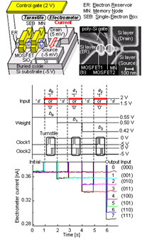 |
||
| K. Nishiguchi, A. Fujiwara, Y. Ono, H. Inokawa, and Y. Takahashi | |||
| [ABSTRACT] A single-electron-based circuit, in which electrons are transferred one by one with a turnstile and subsequently detected with a high-charge-sensitivity electrometer, was fabricated on a silicon-on-insulator substrate. The turnstile, which is operated by opening and closing two metal-oxide-semiconductor field-effect transistors alternately, allows single-electron transfer at room temperature owing to electric-field-assisted shrinkage of the single-electron box. It also achieves fast single-electron transfer (less than 10 ns) and extremely long retention (more than 10^4 s). We have applied these features to a multilevel memory and a time-division weighted sum circuit for a digital-to-analog converter. c 2006 American Institute of Physicsys | |||
| Impurity conduction in phosphorus-doped buried-channel silicon-on-insulator field-effect transistors at temperatures between 10 and 295 K | |||
| Phys. Rev. B, vol. 74, p. 235317 (2006) | |||
| Y. Ono, J-F Morizur, K. Nishiguchi, K. Takashina, and H. Yamaguchi | |||
| [ABSTRACT] We investigate transport in phosphorus-doped buried-channel metal-oxide-semiconductor field-effect transistors at temperatures between 10 and 295 K. We focus on transistors with phosphorus donor concentrations higher than those previously studied, where we expect conduction to rely on donor electrons rather than conduction-band electrons. In a range of doping concentration between around 2.1 and 8.7×10^17 cm^-3, we find that a clear peak emerges in the conductance versus gate-voltage curves at low temperature. In addition, temperature dependence measurements reveal that the conductance obeys a variable-range-hopping law up to an unexpectedly high temperature of over 100 K. The symmetric dual-gate configuration of the silicon-on-insulator we use allows us to fully characterize the vertical-bias dependence of the conductance. Comparison to computer simulation of the phosphorus impurity band depth profile reveals how the spatial variation of the impurity-band energy determines the hopping conduction in transistor structures. We conclude that the emergence of the conductance peak and the high-temperature variable-range hopping originate from the band bending and its change by the gate bias. Moreover, the peak structure is found to be strongly related to the density of states (DOS) of the phosphorus impurity band, suggesting the possibility of performing a spectroscopy for the DOS of phosphorus, the dopant of paramount importance in Si technology, through transport experiments. c 2006 The American Physical Society | |||
| Back-Gate Effect to Coulomb Blockade in Silicon-on-Insulator Trench Wires | |||
| Jpn. J. Appl. Phys., vol. 44, pp. 7717-7719 (2005). | |||
| K. Nishiguchi, C. Olivier, H. Namatsu, S. Horiguchi, Y. Ono, A. Fujiwara, Y. Takahashi, and H. Inokawa | |||
| [ABSTRACT] A back-gate (BG) effect on a Coulomb blockade in a double-gate silicon-on-insulator (SOI) nanowire is investigated. The nanowire, which is situated at the bottom of a trench and connected to thicker source/drain regions, has a naturally formed barrier at both ends and works as a single-electron transistor at low temperatures. We found that a negative BG voltage increases the charging energy of the Coulomb-blockade island in the nanowire as well as the tunnel resistance of the barriers. This indicates the possibility that the BG voltage shifts the electron wave functions in the source/drain area away from the Coulomb-blockade island and decreases the capacitance of the small junctions located at both ends of the island. | |||
| Ballistic Transport in Silicon Nanostructure | |
| Silicon Nanoelectronics ed S. Oda and D. Ferry (Marcel Dekker Inc), p.105 (2005). | |
| H. Mizuta, K. Nishiguchi, and S. Oda | |
| Charge-state control of phosphorous donors in silicon-on-insulator metal-oxide-semiconductor field-effect transistor | |||
| Jpn. J. Appl. Phys., vol. 44, p. 2588 (2005). | |||
| Y. Ono, A. Fujiwara, K. Nishiguchi, H. Inokawa, and Y. Takahashi | |||
| [ABSTRACT] | |||
| Manipulation and detection of single electrons for future information processing | |||
| J. Appl. Phys., vol. 97, p. 031101 (2005). | |||
| Y. Ono, A. Fujiwara, K. Nishiguchi, H. Inokawa, and Y. Takahashi | |||
| [ABSTRACT] The ultimate goal of future information processing might be the realization of a circuit in which one bit is represented by a single electron. Such a challenging circuit would comprise elemental devices whose tasks are to drag, transfer, and detect single electrons. In achieving these tasks, the Coulomb blockade, which occurs in tiny conducting materials, plays an important role. This paper describes the current status of research on such single-charge-control devices from the viewpoints of circuit applications. c 2005 American Institute of Physics | |||
| Multifunctional Boolean Logic Using Single-Electron Transistors | |||
| IEICE Trans. Electron., vol. E87-C, pp. 1809-1817 (2004). | Full adder circuit using single-electron transistors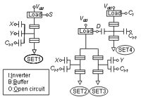 |
||
| K. Nishiguchi, H. Inokawa, Y. Ono, A. Fujiwara, and Y. Takahashi | |||
| [ABSTRACT] A multifunctional Boolean logic circuit composed of single-electron transistors (SETs) was fabricated and its operation demonstrated. The functions of Boolean logic can be changed by the half-period phase shift of the Coulomb-blockade (CB) oscillation of some SETs in the circuit, and an automatic control based on a feedback process is used to attain an exact shift. The amount of charges in the memory node (MN), which is capacitively coupled to the SET, controls the phase of the CB oscillation, and the output signal of the SET controls the amount of charge in the MN during the feedback process. This feedback process automatically adjusts SET output characteristics in such a way that it is used for the multifunctional Boolean logic. We experimentally demonstrated the automatic phase control and examined the speed of the feedback process by SPICE circuit simulation combined with a compact analytical SET model. The simulation revealed that programming time could be of the order of a few ten nanoseconds, thereby promising high-speed switching of the functions of the multifunctional Boolean logic circuit. | |||
| Multilevel memory using an electrically formed single-electron box | |||
| Picked up in August 23, 2004 issue of Virtual Journal of Nanoscale Science & Technology. | |||
| Appl. Phys. Lett., vol. 85, pp. 1277-1279 (2004). | Multileval memory represented by single electrons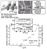 |
||
| K. Nishiguchi, H. Inokawa, Y. Ono, A. Fujiwara, and Y. Takahashi | |||
| [ABSTRACT] A multilevel dynamic random-access memory using a single-electron box (SEB) and single-electron transistor (SET) is fabricated on a silicon-on-insulator substrate. A one-dimensional field-effect transistor (FET), which is connected to the SEB, modulates a barrier potential to precisely control the number of electrons one by one in the SEB by means of the Coulomb-blockade phenomenon. At room temperature and 26 K, we demonstrate a multilevel memory, in which each interval between the levels is given by a single electron, by using the SET electrometer coupled capacitively to the SEB. The control of stored electrons by the FET assures long-retention time and high-speed write/erase operation. | |||
| Multilevel memory using single-electron turnstile | |||
| Electron. Lett., vol. 40, pp. 229-230 (2004). | Single-electron transfer and detection 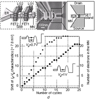 |
||
| K. Nishiguchi, H. Inokawa, Y. Ono, A. Fujiwara, and Y. Takahashi | |||
| [ABSTRACT] A multilevel single-electron memory has been successfully demonstrated. Two fine gates with phase-shifted pulse voltages modulate potential barriers in a one-dimensional Si channel to transfer electrons one by one into a memory node, and the number of electrons in the node is sensed by a single-electron transistor. | |||
| Automatic Control of Oscillation Phase of a Single-Electron Transistor | |||
| IEEE Electron Device Lett. vol. 25, pp. 31-33 (2004). | Control of Coulomb blockade osscilation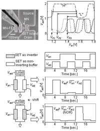 |
||
| K. Nishiguchi, H. Inokawa, Y. Ono, A. Fujiwara, and Y. Takahashi | |||
| [ABSTRACT] Automatic phase control of the Coulomb-blockade (CB) oscillation of a single-electron transistor (SET) is proposed and experimentally demonstrated. Charges in the memory node (MN) capacitively coupled to the SET control the phase of the CB oscillation. The output signal of the SET can controls chares in the MN. This feedback mechanism automatically adjusts the amount of charges, so that the output signal is leveled with a requested one for arbitrary input signal of the SET. The electrical phase control realizes the demonstration of a multifunctional Boolean logic. | |||
| Nanocrystalline silicon electron emitter with a high efficiency enhanced by a planarization technique | |||
| J. Appl. Phys., vol. 92, pp. 2748-2757 (2002). | |||
| K. Nishiguchi, X. Zhao and S. Oda | |||
| [ABSTRACT] A cold electron emitter has been fabricated based on nanocrystalline silicon (nc-Si) quantum dots formed in the gas phase by very-high-frequency plasma decomposition of SiH4. A small size of less than 10 nm and the spherical shape of the nc-Si dots facilitated the generation of hot electrons. Electrons with kinetic energies higher than the work function of the top electrode were extracted into vacuum through the electrode. A planarization process of the nc-Si layer by annealing enhanced the electron emission efficiency to 5%. Efficiency was optimized by varying the thicknesses of the nc-Si layer, the SiO2 layer, and the top electrode film. c 2002 American Institute of Physics. | |||
| Ballistic transport in silicon vertical transistors | |||
| J. Appl. Phys., vol. 92, pp. 1399-1405 (2002). | |||
| K. Nishiguchi and S. Oda | |||
| [ABSTRACT] Clear evidence for ballistic transport has been observed at 5 K from silicon vertical transistors with wrap around gates. The effect of channel shape was investigated experimentally and accounted for theoretically by the anisotropy of the Si conduction band. A reduction in conductance and the appearance of multiple steps were observed when a magnetic field was applied perpendicular to the channel. These results were successfully modeled within the effective mass approximation by including the magnetic vector potential and effects due to series resistance and the spin and valley degeneracy. c 2002 American Institute of Physics. | |||
| A self-aligned two-gate single-electron transistor derived from 0.12μm lithography | |||
| Appl. Phys. Lett., vol. 78, pp. 2070-2072 (2001). | |||
| K. Nishiguchi and S. Oda | |||
| [ABSTRACT] A single-electron transistor (SET) with two gates was fabricated via the self-aligned evaporation of Al into a trench structure comprised of Si and SiO2. The initial trench, which was comparable to 0.12 μm lines and defined by electron-beam lithography, was reduced to 0.05×0.02 μm by a slightly anisotropic etching characteristic. These processes allow for the production of SET devices using current silicon fabrication techniques. The simultaneous formation of two gates allows for one gate to be used to control the background charge of each device. The shift of Coulomb oscillation peaks was clearly shown by controlling the second gate bias. An inverter logic operation at a temperature of 5 K with a gain of 1.3 was obtained. These characteristics indicate that such SET logic devices, based on a combination of the good performance of the Al SET and the high level of control of the fabrication of Si technology, have considerable potential for future use. c 2001 American Institute of Physics. | |||
| Electron transport in a single silicon quantum structure using a vertical silicon probe | |||
| J. Appl. Phys., vol. 88, pp. 4186-4190 (2000). | |||
| K. Nishiguchi and S. Oda | |||
| [ABSTRACT] We present a method of electrical measurement of single nanocrystalline silicon (nc-Si) particles fabricated by plasma-enhanced chemical vapor deposition (CVD) at very high frequency of 144 MHz. A vertical Si probe structure with a spheroidal shaped hole in SiO2 and a CVD grown polycrystalline Si electrode allows stable measurement of current through a single nc-Si quantum dot. Periodic Coulomb staircases are observed between 5 and 50 K. The temperature dependence of the differential conductance is consistent with these being electron transport through a double junction array. A Monte Carlo simulation further supports the double junction array model where a nc-Si quantum dot is covered by 1.5-nm-thick natural oxide as a tunnel barrier. Moreover, applying a wraparound gate makes it possible to observe Coulomb oscillation. c 2000 American Institute of Physics. | |||
| Conductance quantization in nanoscale vertical-structure silicon field-effect transistors with a wrap gate | |||
| Appl. Phys. Lett, vol. 76, pp. 2922-2924 (2000) | |||
| K. Nishiguchi and S. Oda | |||
| [ABSTRACT] Experimental results of quantum ballistic transport in single quantum contact by using vertical structure silicon field effect transistors with a wrap gate are presented. Based on dc measurement, the conductance」oltage characteristics show quantized plateaus at multiples of 2e^2/h. The devices were prepared by electron beam lithography and by combinations of various types of etching. The channel is fabricated by the chemical vapor deposition of amorphous silicon and solid-phase crystallization. The vertical structure allows a channel length as short as 30 nm, which is defined by the film thickness. The effective channel is reduced by the depletion potential, resulting in a much narrower channel width compared to the geometrical width of 60 nm. Thus, the effective size of the silicon transistor is smaller than the elastic mean free path of 40 nm, resulting in the conduction quantization at 3-5 K. c 2000 American Institute of Physics. | |||
| Two-gate transistor for the study of Si/SiO2 interface in silicon-on-insulator nano-channel and nanocrystalline Si memory device | |||
| Jpn. J. Appl. Phys., vol. 39, pp. 4637-4641 (2000) | |||
| B. J. Hinds, K. Nishiguchi, A. Dutta, T. Yamanaka, S. Hatatani, and S. Oda | |||
| [ABSTRACT] A two-gate single electron memory device with active area of 1.5 x 10(-10) cm(2) allows the study of Si/SiO2 interface in nano-scale channels of silicon on insulator (SOI) and nanocrystalline Si (nc-Si) dots. The basis of this device is a trench (150-600 nm wide) defined inside a large "inversion" gate electrode into which nc-Si (8 +/- 1 nm diameter) can be deposited by remote plasma enhanced chemical vapor deposition. Device structure is analyzed with 2-D and 3-D numerical simulation of Poisson's and continuity equations, which show uniform surface potential of channel. The device design allows for tuning of threshold shifts as well as controlling the length of active area from 65-165nm with applied gate bias. This allows for quantifiable threshold shifts for charged interface defects on the channel as well as charge stored in nc-Si. Threshold shifts of between 70-120 mV are calculated depending on the location of charged species along the width of the 30nm wide channel. To study energy levels of single defect sites, lifetime studies of charged sites are possible with and without deposited nc-Si. | |||