| Materials Science Research Laboratory | ||||
| 1 |  |
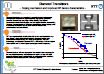
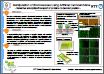
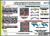
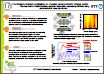
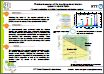
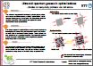
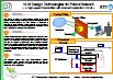
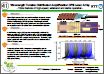
Diamond transistors - Doping mechanism and improved RF device characteristics - |
 |
|
| M. Kasu / M.Kubovic | ||||
| 2 |  |
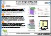
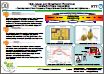
Aluminium nitride light-emitting diodes at 210 nm - Increased emission intensity by non-polar plane - |
 |
|
| Y.Taniyasu / K.Hirama | ||||
| 3 |  |
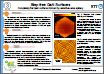
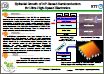
Step-free Gallium nitride grown surface - Atomically flat surface grown by selective growth - |
 |
|
| T.Akasaka | ||||
| 4 |  |
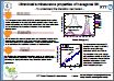
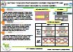
Ultraviolet luminescence of h-BN epitaxial fims - Study of its luminescence mechanism - |
 |
|
| Y.Kobayashi | ||||
| 5 |  |
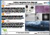
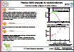
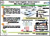
Carbon nanotube growth from diamond - Toward low-cost, large-amount production and structure control of carbon nanotubes - |
 |
|
| D.Takagi | ||||
| 6 |  |
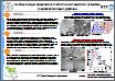
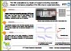
Dependence of structure and electronic properties of epitaxial few-layer graphene on the number of layers |
 |
|
| F.Maeda / H.Hibino | ||||
| 7 |  |
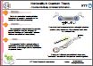
AFM analysis of structural dynamics in receptor - Scientists see receptors open the channel - |
 |
|
| Y.Shinozaki | ||||
| 8 |  |
Examination of reconstituted membrane proteins - Do proteins prefer specific membranes? - |
 |
|
| N.Kasai | ||||
| 9 |  |
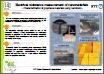
Manipulation of biomolecules using artificial cell membrane - Selective adsorption/transport of proteins to desired position - |
 |
|
| H.Nakashima | ||||
| Physical Science Research Laboratory | ||||
| 10 |  |
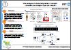
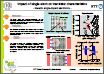
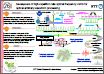
Influence of single atom on transistor characteristics - towards single-dopant electronics - |
 |
|
| Mohammed Khalafalla / Y.Ono | ||||
| 11 |  |
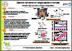
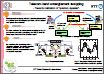
Electron dynamics in single-electron transfer - towards high-accuracy charge manipulation - |
 |
|
| S.Miyamoto / A.Fujiwara | ||||
| 12 |  |
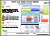
Atomic level design of device materials - Computational experiments - |
 |
|
| H.Kageshima | ||||
| 13 |  |
Compound Semiconductor Mechanical Devices - Highly sensitive detection technique using nano-mechanical vibration - |
 |
|
| H.Okamoto / Imran Mahboob / K.Onomitsu | ||||
| 14 |  |
Electrical resistance measurement of nanomaterials - Evaluation of graphene materials using nanotools - |
 |
|
| M.Nagase | ||||
| 15 |  |
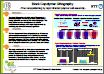
Block Copolymer Lithography - Fine nanopatterning by rapid directed polymer self-assembly - |
 |
|
| T.Yamaguchi | ||||
| 16 |  |
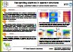
Nanoprobing electrons in quantum structures - Imaging quantized states of semiconductor electrons - |
 |
|
| K.Kanisawa / K.Suzuki | ||||
| 17 |  |
Correlated coherent oscillations in coupled semiconductor charge qubits - Development of multi-functional quantum information processing devices using semiconductor nano-structures - |
 PDF PDF |
|
| T.Ota | ||||
| 18 |  |
NMR study of electronic states in semiconductor quantum structures - Spontaneous breaking of spin symmetry probed by nuclear spins - |
 |
|
| M.Kumada / K.Muraki | ||||
| 19 |  |
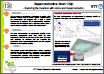
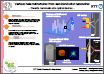
Superconductive Atom Chip - Exploring the Quantum with Atoms and Superconductor - |
 PDF PDF |
|
| T.Mukai | ||||
| 20 |  |
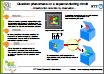
Quantum phenomena in a superconducting circuit - Observation of measurement induced wave packet reduction - |
 |
|
| K.Kakuyanagi | ||||
| 21 |  |
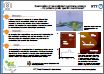
Photoluminescence of the two-dimensional electron system in electric fields - Towards realization of a dilute two-dimensional electron system - |
 |
|
| M.Yamaguchi | ||||
| 22 | |
Evaluation of thin films by means of superconducting resonator - Reveal of thin film properties at microwave frequencies due to superconductivity - |
 |
|
| Y.Harada | ||||
| Optical Science Research Laboratory | ||||
| 23 |  |
Experimental entanglement swapping in the 1.5-um telecom band - Towards realization of quantum repeaters - |
 PDF PDF |
|
| H.Takesue / Miquel / K.Harada | ||||
| 24 | |
Nonlocality in quantum theory - Counterintuitively correlated information - |
 PDF PDF |
|
| F.Morikoshi | ||||
| 25 |  |
Ultracold quantum gases trapped in optical lattices - Challenges to many-body problems via cold atoms - |
 PDF PDF |
|
| K.Inaba / M.Yamashita | ||||
| 26 |  |
Development of high-repetition rate optical frequency comb for optical
arbitrary waveform processing - toward the development of an optical synthesizer - |
 |
|
| T.Nishikawa / A.Ishizawa | ||||
| 27 |  |
Fabrication of various heterostructures from semiconductor nanowires - Toward nanophotonic devices - |
 PDF PDF |
|
| K.Tateno / Guoqiang Zhang | ||||
| 28 |  |
Optical Memory with Extremely-low Energy Consumption - for future optical RAM buffer - |
 PDF PDF |
|
| A.Shinya | ||||
| 29 |  |
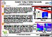
Dynamic Tuning of Optical Nanocavity - Manipulating trapped light - |
 PDF PDF |
|
| H.Taniyama | ||||
| 30 |  |
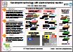
Nanoimprint technology with electrochemical reaction - We can make nano easy - |
 PDF PDF |
|
| A.Yokoo | ||||
| 31 |  |
Nanoimprint technology with electrochemical reaction - Nanoimprint technology with electrochemical reaction - |
 PDF PDF |
|
| A.Takano / T.Makimoto | ||||
| Microsystem Integration Laboratories | ||||
| 32 |  |
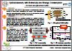
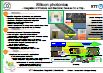
Silicon Photonics - On-chip integration of photonic and electronic devices - |
 |
|
| H.Nishi | ||||
| 33 |  |
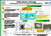
Bio-sensing Technology ~Lab on a Chipによる迅速診断~ |
 |
|
| T.Miura | ||||
| 34 |  |
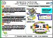
Millimeter- and Terahertz-wave Application Technology - Ultra-high-speed wireless data transmission and millimeter- and terahertz-wave imaging - |
 |
|
| S.Mochizuki / J.Takeuchi / H.Takahashi | ||||
| 35 |  |
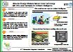
MEMS Devices Technology - Electrochemical technique to control surface tension in micro-structures - |
 |
|
| T.Sakata / J.Ishii | ||||
| 36 |  |
Ultra-lower-energy Wireless Sensor Node Technology - Nano-Watt level Hardware for Ambient Intelligence - |
 |
|
| K.Ono / T.Shimamura | ||||
| 37 |  |
VLSI Desingn Technologies for Future Network - A High-Speed Packet-Filter with Mismatch-Detection Circuit - |
 |
|
| N.Miura | ||||
| Photonics Laboratories | ||||
| 38 |  |
High-power and Broadband Photomixer for Terahertz-Wave Generation - Development of New Frequency Range Between Electric-Waves and Lightwaves - |
 |
|
| A.Wakatsuki / Y.Muramoto / T.Yoshida | ||||
| 39 |  |
Epitaxial growth of InP-based semiconductors for ultra-high-speed electronics |
 |
|
| H.Sugiyama | ||||
| 40 |  |
Low-power-consumption electroabsorption modulator integrated DFB laser - uncooled (cooler less) operation for low power consumption - |
 |
|
| T.Fujisawa / W.Kobayashi / N.Fujiwara | ||||
| 41 |  |
Wavelength tunable distributed amplification DFB laser array - Triple features of Highspeed, wideband and stable operation - |
 |
|
| H.Ishi / N.Nunoya / H.Ohashi | ||||
| 42 |  |
Photonic hybrid integration devices based on silica planar lightwave circuits |
 PDF PDF |
|
| T.Yamada / H.Yamazaki | ||||
| 43 |  |
Hybrid Optoelectronic Router - Large-capacity, low-power router for Green ICT - |
 PDF PDF |
|
| H.Takenouchi | ||||
| 44 |  |
3-D scanner - A Fast 2-D scanner and a varifocal lens made of KTN - |
 PDF PDF |
|
| Y.Sasaki | ||||